|
|
|
PDF LM339 Data sheet ( Hoja de datos )
| Número de pieza | LM339 | |
| Descripción | consists of four independent voltage comparators | |
| Fabricantes | Estek Electronics | |
| Logotipo | ||
 1. Voltage Comparator ( PDF ) Hay una vista previa y un enlace de descarga de LM339 (archivo pdf) en la parte inferior de esta página. Total 6 Páginas | ||
|
No Preview Available !
LM339
Description
The LM339 consists of four independent voltage comparators. These were designed specifically to operate
from a single power supply over a wide range of voltages. Operation from split power supplies is also possible
and the low power supply curr ent drain is independent of the magnitude of the power supply voltage. The
outputs can be connected to other open - collector outputs to achieve wired -AND relationships.
Features
§ Wide supply voltage range
§ Low supply current drain independent of supply voltage.
§ Low input biasing current
§ Low input offset current
§ Low input offset voltage
ww§ w.DInaptauSthceoemt4Um.coonm-mode voltage range includes GND
§ Differential input voltage range equal to the power supply voltage
§ Low output saturation voltage
§ Output voltage compatible with TTL, MOS and CMOS logic
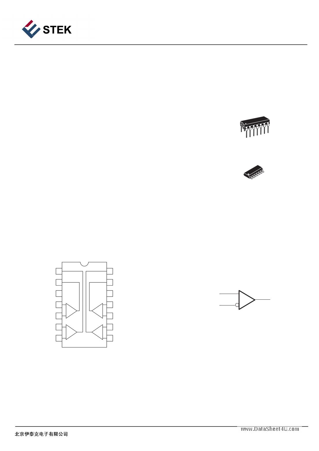
Internal Block Digram
PIN CONNECTIONS
14
1
DIP - 14
14
1
SOP – 14
Package
Output 2 1
Output 1 2
VCC 3
*– Input 1 4
)+ Input 1 5
1
*– Input 2 6
)2
+ Input 2 7
14 Output 3
13 Output 4
12 Gnd
) 11 + Input 4
*4
10 – Input 4
) 9 + Input 3
3*
8 – Input 3
(Top View)
symbol (each comparator)
IN+
OUT
IN–
BEIJING ESTEK ELECTRONICS CO.,LTD
1
1 page 
Typical Applications Circuit
LM339
+ VCC
Vin
+ VCC
R3
10k
Rref
±
+
10k
VO
Vref
10k
R2
R1
1.0M
Vref
≈
VCCR1
Rref+ R1
≈ R1/ / Rref/ / R2
www.DataSheet4U.com
VH =
R1/ / Rref
R1// Rref+R2
[VO(max) -VO(min)]
Rref/ / /R1
Figure 11. Inverting Comparator
with Hystersis
+ VCC
Rref
Vref
10k
R1
Vin
R2
10k
±
+
R3
1.0M
VO
Vref=
VCCR1
Rref+ R1
R2≈ R1/ / Rref
Amount of Hysteresis VH
VH =
R2
R2+ R3
[(VO(max)
-
VO(min)]
Figure 2 . Noninverting Comparator
with Hysteresis
VCC
Vin
V ref
RS +
±
R1
RL
RS =Source Resistance
R1 ≈ RS
Logic
Device
VCC
(V)
CMOS 1/4 MC14001 +15
TTL 1/4 MC7400 +5.0
Figure 3. Driving Logic
RL
kΩ
100
10
VCC. 4.0V
100k
10k
VCC
+
C
R2
330k
R4
R1
±
+
R3
330k
330k
VO
VCC
T1
T2
T1=T2= 0.69RC
f
=
7.2
C(µF)
Figure 4 . Squarewave Oscillator
R2=R3= R4
R2// R3// R4
BEIJING ESTEK ELECTRONICS CO.,LTD
5
5 Page | ||
| Páginas | Total 6 Páginas | |
| PDF Descargar | [ Datasheet LM339.PDF ] | |
Hoja de datos destacado
| Número de pieza | Descripción | Fabricantes |
| LM330 | 3-Terminal Positive Regulator | National Semiconductor |
| LM330-N | LM330 3-Terminal Positive Regulator (Rev. D) | Texas Instruments |
| LM3301 | LM2900/LM3900/LM3301 Quad Amplifiers | National Semiconductor |
| LM3301 | LM2900/LM3900/LM3301 Quad Amplifiers | Texas Instruments |
| Número de pieza | Descripción | Fabricantes |
| SLA6805M | High Voltage 3 phase Motor Driver IC. |
Sanken |
| SDC1742 | 12- and 14-Bit Hybrid Synchro / Resolver-to-Digital Converters. |
Analog Devices |
|
DataSheet.es es una pagina web que funciona como un repositorio de manuales o hoja de datos de muchos de los productos más populares, |
| DataSheet.es | 2020 | Privacy Policy | Contacto | Buscar |