|
|
PDF 49CAZ Data sheet ( Hoja de datos )
| Número de pieza | 49CAZ | |
| Descripción | ISL6549 | |
| Fabricantes | Intersil Corporation | |
| Logotipo |  |
|
Hay una vista previa y un enlace de descarga de 49CAZ (archivo pdf) en la parte inferior de esta página. Total 18 Páginas | ||
|
No Preview Available !
www.DataSheet4U.com
®
Data Sheet
September 22, 2006
ISL6549
FN9168.2
Single 12V Input Supply Dual Regulator —
Synchronous Rectified Buck PWM and
Linear Power Controller
The ISL6549 provides the power control and protection for
two output voltages in high-performance applications. The
dual-output controller drives two N-Channel MOSFETs in a
synchronous rectified buck converter topology and one
N-Channel MOSFET in a linear configuration. The controller is
ideal for applications where regulation of both the processing
unit and memory supplies is required.
The synchronous rectified buck converter incorporates
simple, single feedback loop, voltage-mode control with fast
transient response. Both the switching regulator and linear
regulator provide a maximum static regulation tolerance of
±1% over line, load, and temperature ranges. Each output is
user-adjustable by means of external resistors.
An integrated soft-start feature brings both supplies into
regulation in a controlled manner. Each output is monitored
via the FB pins for undervoltage events. If either output drops
below 75% of the nominal output level, both converters are
shut off and go into retry mode.
The ISL6549 is available in a 14 Ld SOIC package,
16 Ld QSOP, or 16 Ld 4x4 QFN packages.
Related Literature
• Technical Brief TB363 Guidelines for Handling and
Processing Moisture Sensitive Surface Mount Devices
(SMDs)
Ordering Information
Features
• Single 12V bias supply (no 5V supply is required)
• Provides two regulated voltages
- One synchronous rectified buck PWM controller
- One linear controller
• Both controllers drive low cost N-Channel MOSFETs
• Small converter size
- Adjustable frequency 150kHz to 1MHz
- Small external component count
• Excellent output voltage regulation
- Both outputs: ±1% over temperature
• 12V down conversion
• PWM and linear output voltage range: down to 0.8V
• Simple single-loop voltage-mode PWM control design
• Fast PWM converter transient response
- High-bandwidth error amplifier
• Undervoltage fault monitoring on both outputs
• Pb-free plus anneal available (RoHS compliant)
Applications
• Processor and memory supplies
• ASIC power supplies
• Embedded processor and I/O supplies
• DSP supplies
PART NUMBER
PART MARKING
TEMP. RANGE (°C)
PACKAGE
PKG. DWG. #
ISL6549CB
ISL6549CB
0 to 70
14 Ld SOIC
M14.15
ISL6549CBZ (Note)
6549CBZ
0 to 70
14 Ld SOIC (Pb-free)
M14.15
ISL6549CR
ISL6549CR
0 to 70
16 Ld 4x4 QFN
L16.4x4
ISL6549CRZ (Note)
6549CRZ
0 to 70
16 Ld 4x4 QFN (Pb-free)
L16.4x4
ISL6549CA
ISL6549CA
0 to 70
16 Ld QSOP
M16.15A
ISL6549CAZ (Note)
6549CAZ
0 to 70
16 Ld QSOP (Pb-free)
M16.15A
ISL6549CAZA (Note)
6549CAZ
0 to 70
16 Ld QSOP (Pb-free)
M16.15A
ISL6549IBZ (Note)
6549IBZ
-40 to 85
14 Ld SOIC (Pb-free)
M14.15
ISL6549IRZ (Note)
6549IRZ
-40 to 85
16 Ld 4x4 QFN (Pb-free)
L16.4x4
ISL6549IAZ (Note)
6549IAZ
-40 to 85
16 Ld QSOP (Pb-free)
M16.15A
ISL6549LOW-EVAL1
Evaluation Board 1-5A
ISL6549HI-EVAL1
Evaluation Board up to 20A
Add “-T” suffix for tape and reel.
NOTE: Intersil Pb-free plus anneal products employ special Pb-free material sets, molding compounds/die attach materials and 100% matte tin plate
termination finish, which are RoHS compliant and compatible with both SnPb and Pb-free soldering operations. Intersil Pb-free products are MSL
classified at Pb-free peak reflow temperatures that meet or exceed the Pb-free requirements of IPC/JEDEC J STD-020.
1
CAUTION: These devices are sensitive to electrostatic discharge; follow proper IC Handling Procedures.
1-888-INTERSIL or 1-888-468-3774 | Intersil (and design) is a trademark of Intersil Americas Inc.
Copyright © Intersil Americas Inc. 2004, 2006. All Rights Reserved
All other trademarks mentioned are the property of their respective owners.
1 page 
www.DataSheet4U.com
ISL6549
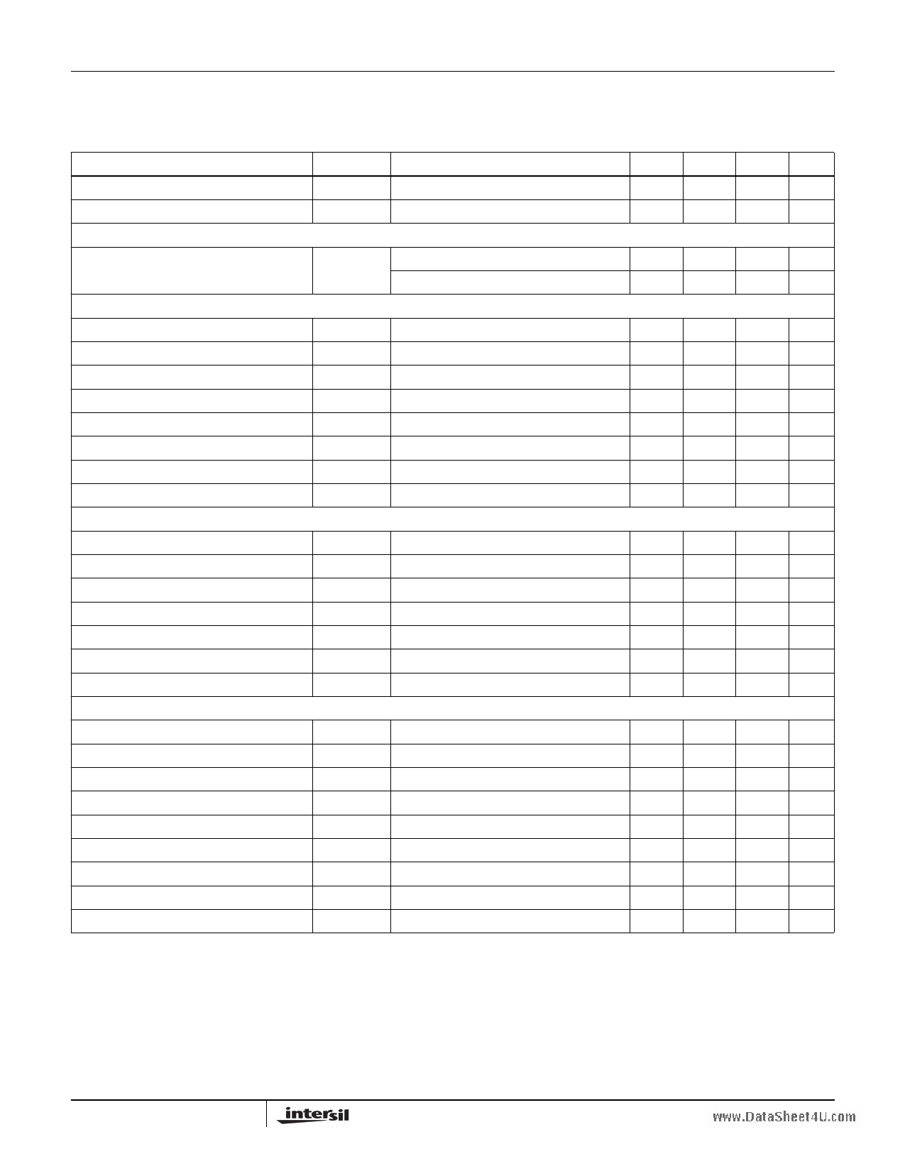
Electrical Specifications
Recommended Operating Conditions, unless otherwise noted. VCC12 = 12V
Temperature = 0 to +70°C (typical = +25°C) for Commercial; Temperature = -40 to + 85°C (typical = +25°C) for
Industrial. Refer to Block Diagram, Simplified Power System Diagram, and Typical Application Schematic.
(Continued)
PARAMETER
SYMBOL
TEST CONDITIONS
MIN TYP MAX UNITS
Sawtooth Amplitude (Note 6)
Soft-Start Interval
REFERENCE VOLTAGE
DVOSC
TSS
FOSC = 620kHz
1.5 V
6.8 ms
Reference Voltage
VREF
ISL6549C; For Error Amp 1 and 2
ISL6549I; For Error Amp 1 and 2
0.792 0.8 0.808 V
0.788 0.8 0.812 V
PWM CONTROLLER ERROR AMPLIFIER
DC Gain (Note 6)
Gain-Bandwidth Product (Note 6)
Slew Rate (Note 6)
FB Input Current
COMP High Output Voltage
COMP Low Output Voltage
COMP High Output, Source Current
Undervoltage Level (VFB/VREF)
PWM CONTROLLER GATE DRIVERS
GBWP
SR
⎜II ⎜
VOUT High
VOUT Low
IOUT High
VUV
RL = 10K, CL = 10pF
RL = 10K, CL = 10pF
RL = 10K, CL = 10pF
VFB = 0.8V
96 dB
20 MHz
8 V/µs
0.1 1.0 µA
4.8 V
0.6 V
-2.8 mA
70 75 80 %
UGATE Maximum Voltage
LGATE Maximum Voltage
UGATE and LGATE Minimum Voltage
UGATE Source Output Impedance
UGATE Sink Output Impedance
LGATE Source Output Impedance
LGATE Sink Output Impedance
LINEAR REGULATOR (LDO_DR)
VHUGATE
VHLGATE
VLGATE
RDS(ON)
RDS(ON)
RDS(ON)
RDS(ON)
VCC12 = 12V; PHASE = 12V
VCC12 = 12V; based on PVCC5 voltage
VCC12 = 12V; PHASE = 0V
VCC12 = 12V; IGATE = 100mA
VCC12 = 12V; IGATE = 100mA
VCC12 = 12V; IGATE = 100mA
VCC12 = 12V; IGATE = 100mA
17 17.5 18
5.25 6
V
0 0.5 V
0.8 Ω
0.7 Ω
0.8 Ω
0.4 Ω
DC Gain (Note 6)
Gain
RL = 10K, CL = 10pF
100 dB
Gain-Bandwidth Product (Note 6)
GBWP RL = 10K, CL = 10pF
2 MHz
Slew Rate (Note 6)
SR RL = 10K, CL = 10pF
6 V/µs
LDO_FB Input Current
⎜II ⎜ VLDO_FB = 0.8V
0.1 1.0 µA
LDO_DR High Output Voltage
VOUT High VCC12 = 12V
11.0 11.5
V
LDO_DR Low Output Voltage
VOUT Low
0.0 0.5 V
LDO_DR High Output Source Current
IOUT High VOUT = 2.0V
2.0 mA
LDO_DR Low Output Sink Current
IOUT Low
0.5 mA
Undervoltage Level (VLDO_FB/VREF)
NOTES:
VUV
Percent of Nominal
70 75 80 %
4. Current in VCC5 is actually higher disabled, due to extra current required to pull down against the FS_DIS pin. VCC12 current is lower disabled.
5. Guaranteed by design, not production tested. Exceeding the maximum current from PVCC5 may result in degraded performance and unsafe
operation.
6. Guaranteed by design, not production tested.
5 FN9168.2
September 22, 2006
5 Page 
www.DataSheet4U.com
ISL6549
C2
COMP
R2 C1
-
E/A +
FB
VREF
R3 C3
R1
Ro
PWM
CIRCUIT
OSCILLATOR
VOSC
HALF-BRIDGE
DRIVE
VIN
UGATE
PHASE
L
LGATE
VOUT
D
C
E
ISL6549 EXTERNAL CIRCUIT
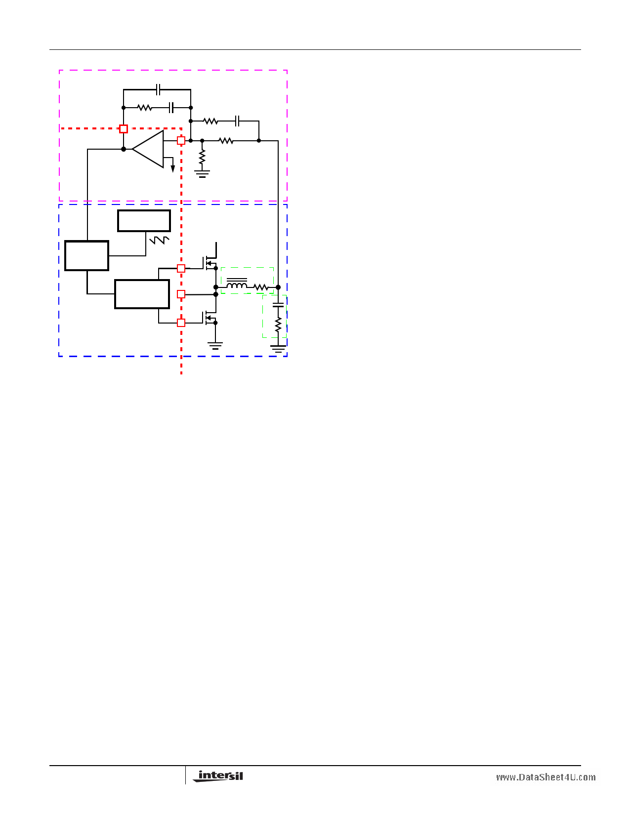
FIGURE 10. VOLTAGE-MODE BUCK CONVERTER
COMPENSATION DESIGN
Use the following guidelines for locating the poles and zeros of
the compensation network:
1. Select a value for R1 (1kΩ to 5kΩ, typically). Calculate
value for R2 for desired converter bandwidth (F0). If
setting the output voltage via an offset resistor connected
to the FB pin, Ro in Figure 10, the design procedure can
be followed as presented.
R2 = d---V-M---O--A---S-X---C--⋅---V⋅---R-I--N--1---⋅--⋅-F--F--L--0-C---
(EQ. 4)
2. Calculate C1 such that FZ1 is placed at a fraction of the FLC,
at 0.1 to 0.75 of FLC (to adjust, change the 0.5 factor to
desired number). The higher the quality factor of the output
filter and/or the higher the ratio FCE/FLC, the lower the FZ1
frequency (to maximize phase boost at FLC).
C1 = -2---π-----⋅---R-----2-----⋅-1--0---.--5-----⋅---F----L---C--
(EQ. 5)
3. Calculate C2 such that FP1 is placed at FCE.
C2 = -2---π-----⋅---R-----2-----⋅---CC-----11----⋅---F----C----E-----–-----1--
(EQ. 6)
4. Calculate R3 such that FZ2 is placed at FLC. Calculate C3
such that FP2 is placed below FSW (typically, 0.5 to 1.0
times FSW). FSW represents the switching frequency.
Change the numerical factor to reflect desired placement
of this pole. Placement of FP2 lower in frequency helps
reduce the gain of the compensation network at high
frequency, in turn reducing the HF ripple component at
the COMP pin and minimizing resultant duty cycle jitter.
R3 = --FF-------S-L------RW--C------1---–----1--
C3 = -2---π-----⋅---R-----3-----⋅--1-0---.--7-----⋅---F----S---W----
(EQ. 7)
It is recommended a mathematical model is used to plot the
loop response. Check the loop gain against the error
amplifier’s open-loop gain. Verify phase margin results and
adjust as necessary. Equation 8 describes the frequency
response of the modulator (GMOD), feedback compensation
(GFB) and closed-loop response (GCL):
GMOD(f) = -d---M---V--A---O-X---S--⋅--C-V----I--N-- ⋅ 1-----+-----s----(--f--)----⋅---(-1-E----+--+---s--D--(--f)--)--⋅--⋅-C--E----+-⋅---C-s---2---(---f--)---⋅---L-----⋅---C---
GFB(f) = s----(-1-f---)-+--⋅---Rs----(-1-f--)--⋅--⋅-(--RC----2-1----⋅-+--C---C--1--2-----) ⋅
⋅ (---1-----+-----s---(---f--)---⋅---R----1-3----+-⋅---C-s---(-3-f--)-)---⋅⋅---⎝⎛(---R1----1+-----+s----(-R-f--)--3--⋅--)-R--⋅---2C----⋅-3--⎝⎛---C--C--------1--1--------+--⋅------C--C--------2--2-----⎠⎞---⎠⎞-
GCL(f) = GMOD(f) ⋅ GFB(f)
where, s(f) = 2π ⋅ f ⋅ j
(EQ. 8)
COMPENSATION BREAK FREQUENCY EQUATIONS
FZ1 = 2----π-----⋅---R---1--2-----⋅---C-----1-
FZ2 = 2----π-----⋅---(---R----1-----+-1----R-----3----)---⋅---C-----3--
FP1 = 2----π-----⋅---R-----2-----⋅1---C--C--------1--1--------+-⋅------C--C--------2--2----
FP2 = 2----π-----⋅---R---1--3-----⋅---C-----3-
(EQ. 9)
Figure 11 shows an asymptotic plot of the DC-DC converter’s
gain vs. frequency. The actual Modulator Gain has a high gain
peak dependent on the quality factor (Q) of the output filter,
which is not shown. Using the above guidelines should yield a
compensation gain similar to the curve plotted. The open loop
error amplifier gain bounds the compensation gain. Check the
compensation gain at FP2 against the capabilities of the error
amplifier. The closed loop gain, GCL, is constructed on the
log-log graph of Figure 11 by adding the modulator gain, GMOD
(in dB), to the feedback compensation gain, GFB (in dB). This is
equivalent to multiplying the modulator transfer function and the
compensation transfer function and then plotting the resulting
gain.
11 FN9168.2
September 22, 2006
11 Page | ||
| Páginas | Total 18 Páginas | |
| PDF Descargar | [ Datasheet 49CAZ.PDF ] | |
Hoja de datos destacado
| Número de pieza | Descripción | Fabricantes |
| 49CAZ | ISL6549 | Intersil Corporation |
| Número de pieza | Descripción | Fabricantes |
| SLA6805M | High Voltage 3 phase Motor Driver IC. |
Sanken |
| SDC1742 | 12- and 14-Bit Hybrid Synchro / Resolver-to-Digital Converters. |
Analog Devices |
|
DataSheet.es es una pagina web que funciona como un repositorio de manuales o hoja de datos de muchos de los productos más populares, |
| DataSheet.es | 2020 | Privacy Policy | Contacto | Buscar |
