|
|
|
PDF RF3166D Data sheet ( Hoja de datos )
| Número de pieza | RF3166D | |
| Descripción | DUAL-BAND GSM900/DCS POWER AMP MODULE | |
| Fabricantes | RF Micro Devices | |
| Logotipo | ||
Hay una vista previa y un enlace de descarga de RF3166D (archivo pdf) en la parte inferior de esta página. Total 12 Páginas | ||
|
No Preview Available !
www.DataSheet4U.com
0
Typical Applications
• 3V Dual-Band GSM Handsets
• Commercial and Consumer Systems
• Portable Battery-Powered Equipment
RF3166D
DUAL-BAND GSM900/DCS
POWER AMP MODULE
• EGSM900/DCS Products
• GPRS Class 12
• Power StarTM Module
Product Description
The RF3166 is a high-power, high-efficiency power ampli-
fier module with integrated power control that provides
over 50dB of control range. The device is a self-contained
6mmx6mm module with 50Ω input and output terminals.
The device is designed for use as the final RF amplifier in
EGSM900 and DCS handheld digital cellular equipment
and other applications in the 880MHz to 915MHz and
1710MHz to 1785MHz bands. The RF3166 incorporates
RFMD’s latest VBATT tracking circuit, which monitors bat-
tery voltage and prevents the power control loop from
reaching saturation. The VBATT tracking circuit eliminates
the need to monitor battery voltage, thereby minimizing
switching transients. The RF3166 requires no external
routing or external components, simplifying layout and
reducing board space.
1.40
1 1.25
6.00
± 0.10
6.00 ± 0.10
Shaded areas represent pin 1.
5.823
5.500
5.400 TYP
5.225 TYP
5.200 TYP
4.625 TYP
4.450 TYP
3.850 TYP
3.675 TYP
3.075 TYP
2.900 TYP
2.300 TYP
2.125 TYP
1.525 TYP
1.350 TYP
0.800 TYP
0.600 TYP
0.500 TYP
0.000
0.450
± 0.075
Dimensions in mm.
1
5.900 TYP
5.435
5.370
5.035
4.600
4.300
4.200
3.800
3.400
3.065
3.000
2.600
2.100
1.700
1.365
1.300
0.900 TYP
0.750 TYP
0.565 TYP
0.100 TYP
Optimum Technology Matching® Applied
Si BJT
9GaAs HBT
GaAs MESFET
Si Bi-CMOS
9SiGe HBT
Si CMOS
InGaP/HBT
GaN HEMT
SiGe Bi-CMOS
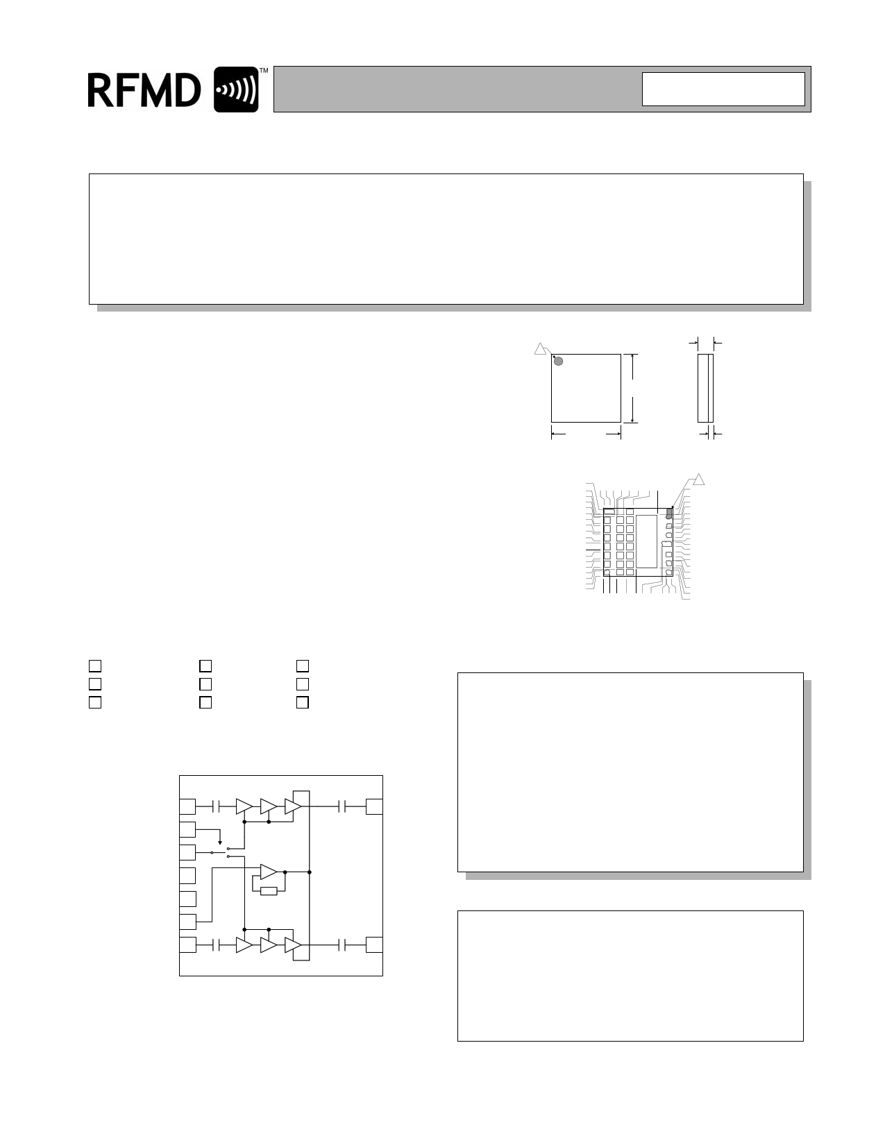
DCS RFIN 1
BAND SELECT 2
TX ENABLE 3
VBATT 4
GND 5
VRAMP 6
GSM
RF IN
7
9
DCS
RFOUT
8
GSM
RFOUT
Functional Block Diagram
Package Style: Module, 6mm x6mm
Features
• Ultra-Small 6mmx6mm Package Size
• Integrated VREG
• Complete Power Control Solution
• Automatic VBATT Tracking Circuit
• No External Components or Routing
• Improved Power Flatness
Ordering Information
RF3166D
Dual-Band GSM900/DCS Power Amp Module
RF3166D SB
Power Amp Module 5-Piece Sample Pack
RF3166DPCBA-410 Fully Assembled Evaluation Board
RF Micro Devices, Inc.
7628 Thorndike Road
Greensboro, NC 27409, USA
Tel (336) 664 1233
Fax (336) 664 0454
http://www.rfmd.com
Rev A2 061006
2-491
1 page 
RF3166D
Pin Function Description
Interface Schematic
1 DCS IN RF input to the DCS band. This is a 50Ω input.
2
BAND
Allows external control to select the GSM or DCS band with a logic high
SELECT
or low. A logic low enables the GSM band whereas a logic high enables BANDSEL
the DCS band.
TXEN
GSMCTRL
DCSCTRL
3 TX ENABLE This signal enables the PA module for operation with a logic high.
VBATT
TX EN
TX ON
4
VBATT
Power supply for the module. This should be connected to the battery.
5 GND
6 VRAMP Ramping signal from DAC. A 300kHz lowpass filter is integrated into
the CMOS. No external filtering is required.
7
8
9
Pkg
Base
GSM IN
GSM OUT
DCS/PCS
OUT
GND
RF input to the GSM band. This is a 50Ω input.
RF output for the GSM band. This is a 50Ω output. The output load line
matching is contained internal to the package.
RF output for the DCS band. This is a 50Ω output. The output load line
matching is contained internal to the package.
VRAMP
300 kHz
Rev A2 061006
2-495
5 Page 
RF3166D
An often overlooked problem in PA control loops is that a delay not only decreases loop stability it also affects the burst
timing when, for instance the input power from the VCO decreases (or increases) with respect to temperature or supply
voltage. The burst timing then appears to shift to the right especially at low power levels. The RF3166 is insensitive to a
change in input power and the burst timing is constant and requires no software compensation.
Switching transients occur when the up and down ramp of the burst is not smooth enough or suddenly changes shape. If
the control slope of a PA has an inflection point within the output power range or if the slope is simply too steep it is diffi-
cult to prevent switching transients. Controlling the output power by changing the collector voltage is as earlier described
based on the physical relationship between voltage swing and output power. Furthermore all stages are kept constantly
biased so inflection points are nonexistent.
Harmonics are natural products of high efficiency power amplifier design. An ideal class “E” saturated power amplifier
will produce a perfect square wave. Looking at the Fourier transform of a square wave reveals high harmonic content.
Although this is common to all power amplifiers, there are other factors that contribute to conducted harmonic content as
well. With most power control methods a peak power diode detector is used to rectify and sense forward power. Through
the rectification process there is additional squaring of the waveform resulting in higher harmonics. The RF3166 address
this by eliminating the need for the detector diode. Therefore the harmonics coming out of the PA should represent the
maximum power of the harmonics throughout the transmit chain. This is based upon proper harmonic termination of the
transmit port. The receive port termination on the T/R switch as well as the harmonic impedance from the switch itself
will have an impact on harmonics. Should a problem arise, these terminations should be explored.
Rev A2 061006
2-501
11 Page | ||
| Páginas | Total 12 Páginas | |
| PDF Descargar | [ Datasheet RF3166D.PDF ] | |
Hoja de datos destacado
| Número de pieza | Descripción | Fabricantes |
| RF3166 | POWER AMPLIFIER MODULE | RF Micro Devices |
| RF3166D | DUAL-BAND GSM900/DCS POWER AMP MODULE | RF Micro Devices |
| Número de pieza | Descripción | Fabricantes |
| SLA6805M | High Voltage 3 phase Motor Driver IC. |
Sanken |
| SDC1742 | 12- and 14-Bit Hybrid Synchro / Resolver-to-Digital Converters. |
Analog Devices |
|
DataSheet.es es una pagina web que funciona como un repositorio de manuales o hoja de datos de muchos de los productos más populares, |
| DataSheet.es | 2020 | Privacy Policy | Contacto | Buscar |