|
|
|
PDF ISL97650 Data sheet ( Hoja de datos )
| Número de pieza | ISL97650 | |
| Descripción | 4-Channel Integrated LCD Supply | |
| Fabricantes | Intersil Corporation | |
| Logotipo | ||
Hay una vista previa y un enlace de descarga de ISL97650 (archivo pdf) en la parte inferior de esta página. Total 20 Páginas | ||
|
No Preview Available !
®
Data Sheet
November 28, 2006
ISL97650
FN9198.3
4-Channel Integrated LCD Supply
The ISL97650 represents a high power, integrated LCD
supply IC targeted at large panel LCD displays. The
ISL97650 integrates a high power, 2.6A boost converter for
AVDD generation, an integrated VON charge pump, a VOFF
charge pump driver, VON slicing circuitry and a buck
regulator with 2A switch for logic generation.
The ISL97650 has been designed for ease of layout and low
BOM cost. Supply sequencing is integrated for both
AVDD -> VOFF -> VON and AVDD/VOFF -> VON sequences.
The TFT power sequence uses a separate enable to the
logic buck regulator for maximum flexibility.
Peak efficiencies are >90% for both the boost and buck while
operating from a 4V to 14V input supply. The current mode
buck offers superior line and load regulation. Available in the
36 Ld QFN package, the ISL97650 is specified for ambient
operation over the -40°C to +105°C temperature range.
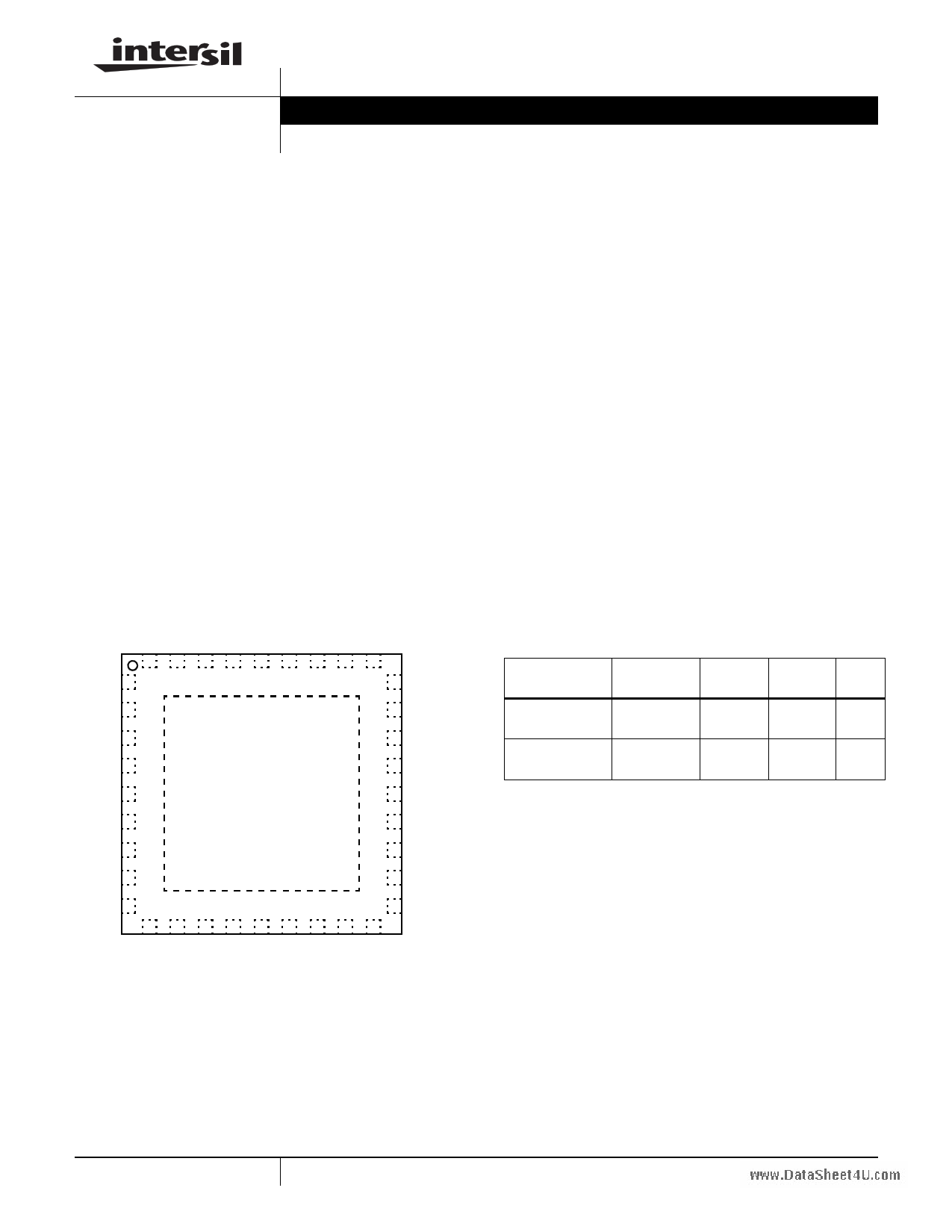
Pinout
ISL97650
(36 LD TQFN)
TOP VIEW
LX1 1
LX2 2
CB 3
LXL 4
NC 5
VSUP 6
FBL 7
CM2 8
CTL 9
THERMAL
PAD
27 AGND1
26 PGND1
25 PGND2
24 VINL
23 NOUT
22 PGND3
21 FBN
20 VREF
19 FBP
Features
• 4V to 14V input supply
• AVDD boost up to 20V, with integrated 2.8A FET
• Integrated VON charge pump, up to 35V out
• VOFF charge pump driver, down to -18V
• VLOGIC buck down to 1.2V, with integrated 2A FET
• Automatic start-up sequencing
- AVDD -> VOFF -> VON or AVDD/VOFF -> VON
- Independent logic enable
• VON slicing
• Thermally enhanced 6x6 Thin QFN package
• Pb-free plus anneal available (RoHS compliant)
Applications
• LCD monitors (15”+)
• LCD-TVs (up to 40”)
• Notebook displays (up to 16”)
• Industrial/medical LCD displays
Ordering Information
PART NUMBER
PART
(Note)
MARKING
TAPE & PACKAGE PKG.
REEL (Pb-Free) DWG. #
ISL97650ARTZ-T ISL97650ARTZ 13” (4k pcs) 36 Ld 6x6 L36.6x6
Thin QFN
ISL97650ARTZ-TK ISL97650ARTZ 13” (1k pcs) 36 Ld 6x6 L36.6x6
Thin QFN
NOTE: Intersil Pb-free plus anneal products employ special Pb-free
material sets; molding compounds/die attach materials and 100%
matte tin plate termination finish, which are RoHS compliant and
compatible with both SnPb and Pb-free soldering operations. Intersil
Pb-free products are MSL classified at Pb-free peak reflow
temperatures that meet or exceed the Pb-free requirements of
IPC/JEDEC J STD-020.
1 CAUTION: These devices are sensitive to electrostatic discharge; follow proper IC Handling Procedures.
1-888-INTERSIL or 1-888-468-3774 | Intersil (and design) is a registered trademark of Intersil Americas Inc.
Copyright Intersil Americas Inc. 2006. All Rights Reserved
All other trademarks mentioned are the property of their respective owners.
1 page 
ISL97650
Electrical Specifications VIN = 12V, VBOOST = VSUP = 15V, VON = 25V, VOFF = -8V, over temperature from -40°C to +105°C, unless
otherwise stated. (Continued)
PARAMETER
DESCRIPTION
CONDITIONS
MIN TYP MAX UNIT
Vth_POUT(FBP)
Vth_NOUT(FBN)
TFD
POUT Charge Pump Short Detection
NOUT Charge Pump Short Detection
Fault Delay Time to Chip Turns Off
V(FBP) falling less than
V(FBN) rising more than
0.9 V
0.4 V
52 ms
START-UP SEQUENCING
tSTART-UP
IDELB_ON
Enable to AVDD Start Time
CDEL = 220nF
DELB Pull-Down Current or Resistance VDELB > 0.9V
when Enabled by the Start-Up Sequence
VDELB < 0.9V
80
36 50 70
1.00 1.326 1.75
ms
µA
kΩ
IDELB_OFF
DELB Pull-Down Current or Resistance VDELB < 20V
when Disabled
500 nA
CDEL
Sequence Timing and Fault Time Out
Capacitor
10 220 nF
tVOFF
tVON
tVON-SLICE
AVDD to VOFF
VOFF to VON Delay
VON to VON-SLICE Delay
CDEL = 220nF
CDEL = 220nF
CDEL = 220nF
9 ms
20 ms
17 ms
Typical Performance Curves
100
VIN = 12V
80
VIN = 5V
60
40
20
0.12
0.1
0.08
0.06
0.04
0.02
VIN = 5V
VIN = 12V
0
0 500 1000
IO (mA)
FIGURE 1. BOOST EFFICIENCY
1500
0
0
500
1000
1500
IO (mA)
FIGURE 2. BOOST LOAD REGULATION
2000
100
VIN = 5V
80
VIN = 12V
60
40
20
0
0
500
1000
1500
IO (mA)
FIGURE 3. BUCK EFFICIENCY
2000
0
-0.5
VIN = 5V
VIN = 12V
-1.0
-1.5
-2.0
0
500
1000
1500
IO (mA)
FIGURE 4. BUCK LOAD REGULATION
2000
5 FN9198.3
November 28, 2006
5 Page 
ISL97650
Applications Information
The ISL97650 provides a complete power solution for TFT
LCD applications. The system consists of one boost
converter to generate AVDD voltage for column drivers, one
buck converter to provide voltage to logic circuit in the LCD
panel, one integrated VON charge pump and one VOFF
linear-regulator controller to provide the voltage to row
drivers. This part also integrates VON-slice circuit which can
help to optimize the picture quality. With the high output
current capability, this part is ideal for big screen LCD TV
and monitor panel application.
The integrated boost converter and buck converter operate
at 1.2MHz which can allow to use multilayer ceramic
capacitors and low profile inductor which result in low cost,
compact and reliable system. The logic output voltage is
independently enabled to give flexibility to the system
designers.
Boost Converter
The boost converter is a current mode PWM converter
operating at a fixed frequency of 1.2MHz. It can operate in
both discontinuous conduction mode (DCM) at light load and
continuous mode (CCM). In continuous current mode,
current flows continuously in the inductor during the entire
switching cycle in steady state operation. The voltage
conversion ratio in continuous current mode is given by:
V-----b---o---o----s---t
VIN
=
------1-------
1–D
(EQ. 1)
Where D is the duty cycle of the switching MOSFET.
The boost converter uses a summing amplifier architecture
consisting of gm stages for voltage feedback, current
feedback and slope compensation. A comparator looks at
the peak inductor current cycle by cycle and terminates the
PWM cycle if the current limit is reached.
An external resistor divider is required to divide the output
voltage down to the nominal reference voltage. Current
drawn by the resistor network should be limited to maintain
the overall converter efficiency. The maximum value of the
resistor network is limited by the feedback input bias current
and the potential for noise being coupled into the feedback
pin. A resistor network in the order of 60kΩ is recommended.
The boost converter output voltage is determined by the
following equation:
AVDD
=
R-----3-----+----R-----5-
R5
×
VF
B
B
(EQ. 2)
The current through the MOSFET is limited to 2.6Apeak.
This restricts the maximum output current (average) based
on the following equation:
IOMAX
=
⎛
⎝
IL
M
T
–
-Δ--2--I-L--⎠⎞
×
V-----I--N--
VO
(EQ. 3)
Where ΔIL is peak to peak inductor ripple current, and is set
by:
ΔIL
=
-V----I--N-- × -D---
L fS
(EQ. 4)
where fs is the switching frequency(1.2MHz).
The following table gives typical values (margins are
considered 10%, 3%, 20%, 10% and 15% on VIN, VO, L, fs
and IOMAX):
TABLE 1. MAXIMUM OUTPUT CURRENT CALCULATION
VIN (V)
5
VO (V)
9
L (µH)
6.8
fs (MHz)
1.2
IOMAX (mA)
1138
5
12 6.8 1.2
777
4
15 6.8 1.2
560
12 15 6.8 1.2 1345
12 18 6.8 1.2 998
The minimum duty cycle of the ISL97650 is 25%. When the
operating duty cycle is lower than the minimum duty cycle,
the part will not switch in some cycles randomly, which will
cause some LX pulses to be skipped. In this case, LX pulses
are not consistent any more, but the output voltage (AVDD) is
still regulated by the ratio of R3 and R5. This relationship is
given by Equation 2. Because some LX pulses are skipped,
the ripple current in the inductor will become bigger. Under
the worst case, the ripple current will be from 0 to the
threshold of the current limit. In turn, the bigger ripple current
will increase the output voltage ripple. Hence, it will need
more output capacitors to keep the output ripple at the same
level. When the input voltage equals, or is larger than, the
output voltage, the boost converter will stop switching. The
boost converter is not regulated any more, but the part will
still be on and other channels are still regulated. The typical
waveforms of pulse-skipping mode are shown in the "Typical
Performance Curves" section.
Boost Converter Input Capacitor
An input capacitor is used to suppress the voltage ripple
injected into the boost converter. The ceramic capacitor with
capacitance larger than 10µF is recommended. The voltage
rating of input capacitor should be larger than the maximum
input voltage. Some capacitors are recommended in Table 2
for input capacitor.
TABLE 2. BOOST CONVERTER INPUT CAPACITOR
RECOMMENDATION
CAPACITOR SIZE
VENDOR
PART NUMBER
10µF/25V 1210 TDK
C3225X7R1E106M
10µF/25V 1210 Murata
GRM32DR61E106K
11 FN9198.3
November 28, 2006
11 Page | ||
| Páginas | Total 20 Páginas | |
| PDF Descargar | [ Datasheet ISL97650.PDF ] | |
Hoja de datos destacado
| Número de pieza | Descripción | Fabricantes |
| ISL97650 | 4-Channel Integrated LCD Supply | Intersil Corporation |
| ISL97650B | 4-Channel Integrated LCD Supply | Intersil Corporation |
| ISL97651 | 4-Channel Integrated LCD Supply | Intersil Corporation |
| ISL97652 | 4-Channel Integrated LCD Supply | Intersil Corporation |
| Número de pieza | Descripción | Fabricantes |
| SLA6805M | High Voltage 3 phase Motor Driver IC. |
Sanken |
| SDC1742 | 12- and 14-Bit Hybrid Synchro / Resolver-to-Digital Converters. |
Analog Devices |
|
DataSheet.es es una pagina web que funciona como un repositorio de manuales o hoja de datos de muchos de los productos más populares, |
| DataSheet.es | 2020 | Privacy Policy | Contacto | Buscar |