|
|
PDF ISL6441 Data sheet ( Hoja de datos )
| Número de pieza | ISL6441 | |
| Descripción | Step-Down PWM and Single Linear Controller | |
| Fabricantes | Intersil Corporation | |
| Logotipo |  |
|
Hay una vista previa y un enlace de descarga de ISL6441 (archivo pdf) en la parte inferior de esta página. Total 18 Páginas | ||
|
No Preview Available !
®
Data Sheet
October 4, 2005
ISL6441
FN9197.1
1.4MHz Dual, 180° Out-of-Phase, Step-
Down PWM and Single Linear Controller
The ISL6441 is a high-performance, triple-output controller
optimized for converting wall adapter, battery or network
intermediate bus DC input supplies into the system supply
voltages required for a wide variety of applications. Each
output is adjustable down to 0.8V. The two PWMs are
synchronized 180o out of phase reducing the RMS input
current and ripple voltage.
The ISL6441 incorporates several protection features. An
adjustable overcurrent protection circuit monitors the output
current by sensing the voltage drop across the lower
MOSFET. Hiccup mode overcurrent operation protects the
DC/DC components from damage during output
overload/short circuit conditions. Each PWM has an
independent logic-level shutdown input (SD1 and SD2).
A single PGOOD signal is issued when soft-start is complete
on both PWM controllers and their outputs are within 10% of
the set point and the linear regulator output is greater than
75% of its setpoint. Thermal shutdown circuitry turns off the
device if the junction temperature exceeds +150°C.
Ordering Information
PART
PART
NUMBER MARKING
TEMP.
RANGE
(°C)
PACKAGE
PKG.
DWG. #
ISL6441IR ISL6441IR -40 to 85 28 Ld QFN L28.5x5
ISL6441IRZ ISL6441IRZ -40 to 85 28 Ld QFN L28.5x5
(See Note)
(Pb-free)
Add “-T” or “-TK” suffix to part number for tape and reel packaging.
NOTE: Intersil Pb-free plus anneal products employ special Pb-free
material sets; molding compounds/die attach materials and 100%
matte tin plate termination finish, which are RoHS compliant and
compatible with both SnPb and Pb-free soldering operations. Intersil
Pb-free products are MSL classified at Pb-free peak reflow
temperatures that meet or exceed the Pb-free requirements of
IPC/JEDEC J STD-020.
Features
• Wide Input Supply Voltage Range
- 5.6V to 24V
- 4.5V to 5.6V
• Three Independently Programmable Output Voltages
• Switching Frequency . . . . . . . . . . . . . . . . . . . . . . .1.4MHz
• Out of Phase PWM Controller Operation
- Reduces Required Input Capacitance and Power
Supply Induced Loads
• No External Current Sense Resistor
- Uses Lower MOSFET’s rDS(ON)
• Bi-directional Frequency Synchronization for
Synchronizing Multiple ISL6441s
• Programmable Soft-Start
• Extensive Circuit Protection Functions
- PGOOD
- UVLO
- Overcurrent
- Overtemperature
- Independent Shutdown for Both PWMs
• Excellent Dynamic Response
- Voltage Feed-Forward with Current Mode Control
• QFN Package:
- QFN - Compliant to JEDEC PUB95 MO-220
QFN - Quad Flat No Leads - Package Outline
- Near Chip Scale Package footprint, which improves
PCB efficiency and has a thinner profile
• Pb-Free Plus Anneal Available (RoHS Compliant)
Applications
• Power Supplies with Multiple Outputs
• xDSL Modems/Routers
• DSP, ASIC, and FPGA Power Supplies
• Set-Top Boxes
• Dual Output Supplies for DSP, Memory, Logic, µP Core
and I/O
• Telecom Systems
1
CAUTION: These devices are sensitive to electrostatic discharge; follow proper IC Handling Procedures.
1-888-INTERSIL or 1-888-468-3774 | Intersil (and design) is a registered trademark of Intersil Americas Inc.
Copyright © Intersil Americas Inc. 2004, 2005. All Rights Reserved
All other trademarks mentioned are the property of their respective owners.
1 page 
ISL6441
Absolute Maximum Ratings
Supply Voltage (VCC_5V Pin) . . . . . . . . . . . . . . . . . . . . -0.3V to +7V
Input Voltage (VIN Pin) . . . . . . . . . . . . . . . . . . . . . . . . . . . . . . .+27V
BOOT1, 2 and UGATE1, 2. . . . . . . . . . . . . . . . . . . . . . . . . . . . +35V
PHASE1, 2 and ISEN1, 2 . . . . . . . . . . . . . . . . . . . . . . . . . . . . +27V
BOOT1, 2 with Respect to PHASE1, 2 . . . . . . . . . . . . . . . . . . +6.5V
UGATE1, 2. . . . . . . . . . . . (PHASE1, 2 - 0.3V) to (BOOT1, 2 +0.3V)
Thermal Information
Thermal Resistance (Typical)
θJA (°C/W) θJC (°C/W)
28 Lead QFN (Note 1) . . . . . . . . . . .
36
5.5
Maximum Junction Temperature (Plastic Package) . -55°C to 150°C
Maximum Storage Temperature Range . . . . . . . . . . . -65°C to 150°C
Temperature Range . . . . . . . . . . . . . . . . . . . . . . . . . . . -40°C to 85°C
CAUTION: Stresses above those listed in “Absolute Maximum Ratings” may cause permanent damage to the device. This is a stress only rating and operation of the
device at these or any other conditions above those indicated in the operational sections of this specification is not implied.
NOTE:
1. θJC is measured in free air with the component mounted on a high effective thermal conductivity test board with “direct attach” features. For θJA
the “case temp” location is the center of the exposed metal pad on the underside of the package. See Tech Brief TB379.
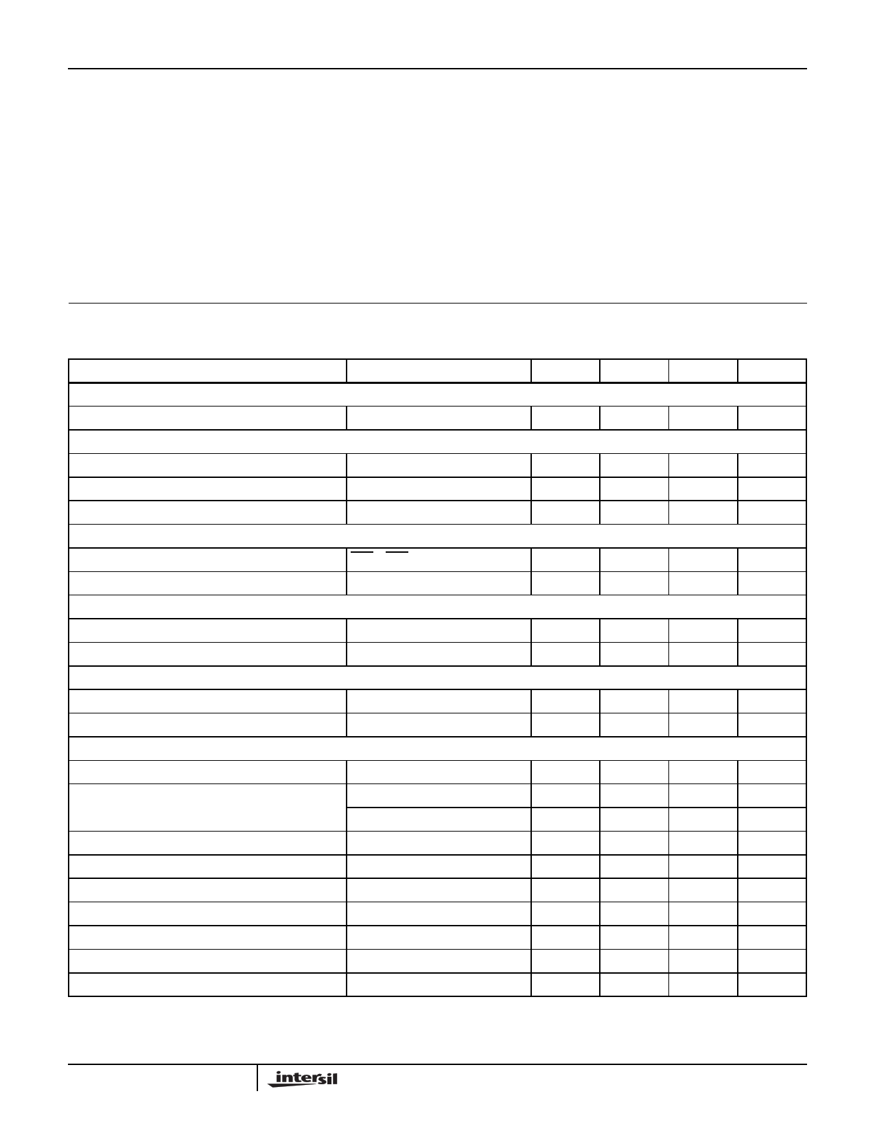
Electrical Specifications
Recommended operating conditions unless otherwise noted. Refer to Block Diagram and Typical Application
Schematic. VIN = 5.6V to 24V, or VCC_5V = 5V ±10%, TA = -40°C to 85°C (Note 2),
Typical values are at TA = 25°C
PARAMETER
TEST CONDITIONS
MIN
TYP
MAX
UNITS
VIN SUPPLY
Input Voltage Range
5.6 12
24
V
VCC_5V SUPPLY (Note 3)
Input Voltage
VIN = VCC_5V
4.5 5.0 5.6
V
Output Voltage
Maximum Output Current
SUPPLY CURRENT
VIN > 5.6V, IL = 20mA
VIN = 12V
4.5 5.0 5.5
V
60 -
- mA
Shutdown Current (Note 4)
SD1 = SD2 = GND
- 50 375 µA
Operating Current (Note 5)
- 2.0 4.0 mA
REFERENCE SECTION
Nominal Reference Voltage
- 0.8 -
V
Reference Voltage Tolerance
-1.0 - 1.0 %
POWER-ON RESET
Rising VCC_5V Threshold
4.25 4.45
4.5
V
Falling VCC_5V Threshold
3.95 4.2
4.4
V
OSCILLATOR
Total Frequency Variation
1.25 1.4 1.55 MHz
Peak-to-Peak Sawtooth Amplitude (Note 6)
Ramp Offset (Note 7)
VIN = 12V
VIN = 5V
- 1.5 -
- 0.625 -
- 1.0 -
V
V
V
SYNC Input Rise/Fall Time (Note 7)
- - 10.0 ns
SYNC Frequency Range
5.1 5.6 6.2 MHz
SYNC Input HIGH Level
3.5 - - V
SYNC Input LOW Level
- - 1.5 V
SYNC Input Minimum Pulse Width (Note 7)
10 -
- ns
SYNC Output HIGH Level
VCC - 0.6V
-
-
V
5 FN9197.1
October 4, 2005
5 Page 
ISL6441
For example, a single large FET with 15nC total gate charge
requires 15nC X 1.4MHz = 21mA. Also, at higher input
voltages with larger FETs, the power dissipation across the
internal 5V will increase. Excessive dissipation across this
regulator must be avoided to prevent junction temperature
rise. Larger FETs can be used with 5V ±10% input
applications. The thermal overload protection circuit will be
triggered if the VCC_5V output is short circuited. Connect
VCC_5V to VIN for 5V ±10% input applications.
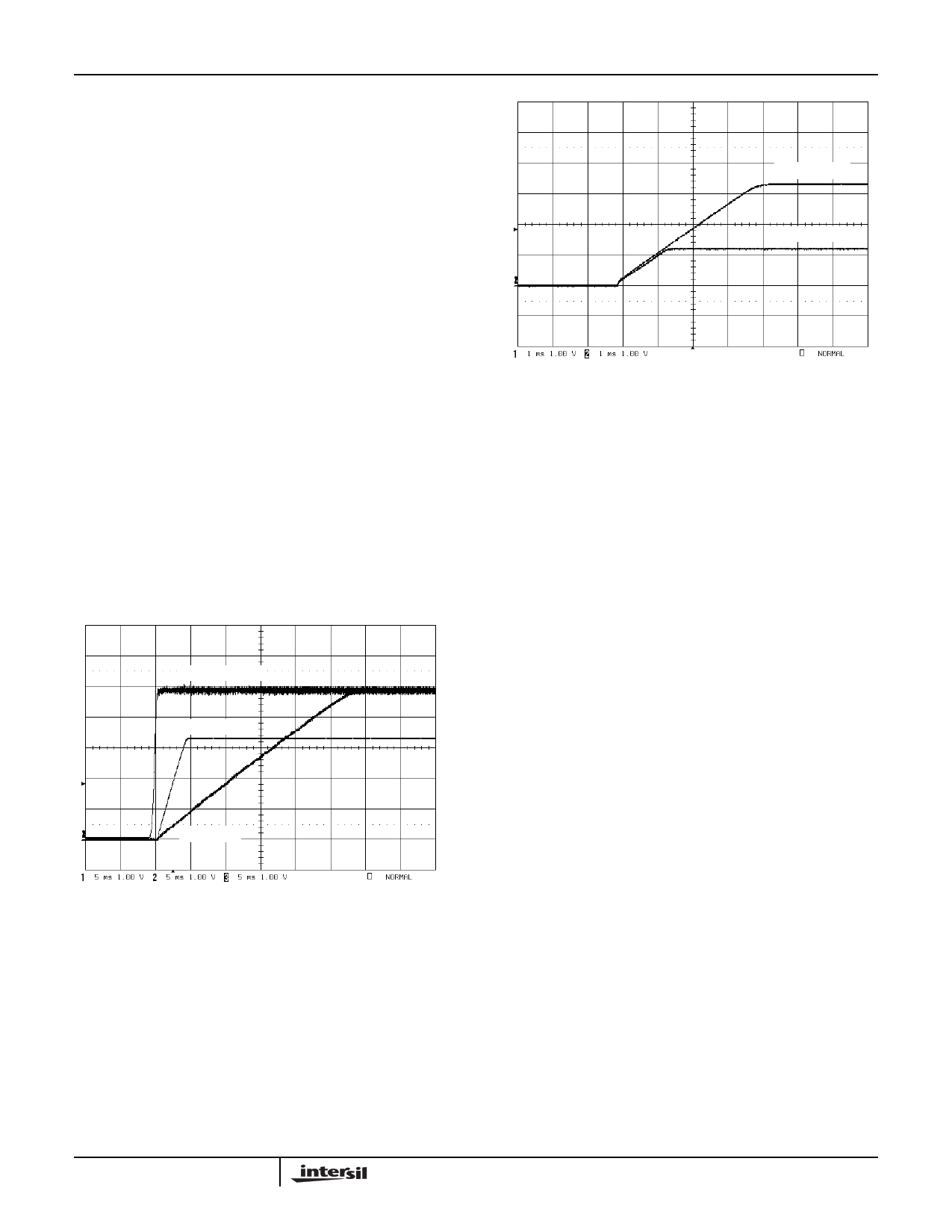
Soft-Start Operation
When soft-start is initiated, the voltage on the SS pin of the
enabled PWM channels starts to ramp gradually, due to the
5µA current sourced into the external capacitor. The output
voltage follows the soft-start voltage.
When the SS pin voltage reaches 0.8V, the output voltage of
the enabled PWM channel reaches the regulation point, and
the soft-start pin voltage continues to rise. At this point the
PGOOD and fault circuitry is enabled. This completes the
soft-start sequence. Any further rise of SS pin voltage does
not affect the output voltage. By varying the values of the
soft-start capacitors, it is possible to provide sequencing of the
main outputs at start-up. The soft-start time can be obtained
from the following equation:
TSOFT
=
0.8
V
-C5---µ-S---A-S--
VCC_5V 1V/DIV
VOUT1 1V/DIV
SS1 1V/DIV
FIGURE 13. SOFT-START OPERATION
The soft-start capacitors can be chosen to provide startup
tracking for the two PWM outputs. This can be achieved by
choosing the soft-start capacitors such that the soft-start
capacitor ration equals the respective PWM output voltage
ratio. For example, if I use PWM1 = 1.2V and PWM2 = 3.3V
then the soft-start capacitor ration should be,
CSS1/CSS1 = 1.2/3.3 = 0.364. Figure 14 shows that soft-start
waveform with CSS1 = 0.01µF and CSS2 = 0.027µF.
VOUT1 1V/DIV
VOUT2 1V/DIV
FIGURE 14. PWM1 AND PWM2 OUTPUT TRACKING DURING
STARTUP
Output Voltage Programming
A resistive divider from the output to ground sets the output
voltage of either PWM channel. The center point of the
divider shall be connected to FBx pin. The output voltage
value is determined by the following equation.
VOUTx
=
0.8
V
R-----1---R--+---2--R-----2--
where R1 is the top resistor of the feedback divider network
and R2 is the resistor connected from FBx to ground.
Out-of-Phase Operation
The two PWM controllers in the ISL6441 operate 180o out-
of-phase to reduce input ripple current. This reduces the
input capacitor ripple current requirements, reduces power
supply-induced noise, and improves EMI. This effectively
helps to lower component cost, save board space and
reduce EMI.
Dual PWMs typically operate in-phase and turn on both
upper FETs at the same time. The input capacitor must then
support the instantaneous current requirements of both
controllers simultaneously, resulting in increased ripple
voltage and current. The higher RMS ripple current lowers
the efficiency due to the power loss associated with the ESR
of the input capacitor. This typically requires more low-ESR
capacitors in parallel to minimize the input voltage ripple and
ESR-related losses, or to meet the required ripple current
rating.
With dual synchronized out-of-phase operation, the high-
side MOSFETs of the ISL6441 turn on 180o out-of-phase.
The instantaneous input current peaks of both regulators no
longer overlap, resulting in reduced RMS ripple current and
input voltage ripple. This reduces the required input
capacitor ripple current rating, allowing fewer or less
expensive capacitors, and reducing the shielding
requirements for EMI. The typical operating curves show the
synchronized 180° out-of-phase operation.
11 FN9197.1
October 4, 2005
11 Page | ||
| Páginas | Total 18 Páginas | |
| PDF Descargar | [ Datasheet ISL6441.PDF ] | |
Hoja de datos destacado
| Número de pieza | Descripción | Fabricantes |
| ISL644 | High Voltage ORing MOSFET Controller | Intersil |
| ISL6440 | Step-Down PWM Controller | Intersil Corporation |
| ISL6440A | Advanced PWM and Triple Linear Power Controller | Intersil Corporation |
| ISL6441 | Step-Down PWM and Single Linear Controller | Intersil Corporation |
| Número de pieza | Descripción | Fabricantes |
| SLA6805M | High Voltage 3 phase Motor Driver IC. |
Sanken |
| SDC1742 | 12- and 14-Bit Hybrid Synchro / Resolver-to-Digital Converters. |
Analog Devices |
|
DataSheet.es es una pagina web que funciona como un repositorio de manuales o hoja de datos de muchos de los productos más populares, |
| DataSheet.es | 2020 | Privacy Policy | Contacto | Buscar |
