|
|
|
PDF ISL8703A Data sheet ( Hoja de datos )
| Número de pieza | ISL8703A | |
| Descripción | (ISL8700A - ISL8705A) Adjustable Quad Sequencer | |
| Fabricantes | Intersil Corporation | |
| Logotipo | ||
Hay una vista previa y un enlace de descarga de ISL8703A (archivo pdf) en la parte inferior de esta página. Total 12 Páginas | ||
|
No Preview Available !
®
Data Sheet
ISL8700A, ISL8701A, ISL8702A,
ISL8703A, ISL8704A, ISL8705A
October 12, 2006
FN6381.0
Adjustable Quad Sequencer
The ISL8700A, ISL8701A, ISL8702A, ISL8703A, ISL8704A,
ISL8705A family of ICs provide four delay adjustable
sequenced outputs while monitoring an input voltage all with
a minimum of external components.
High performance DSP, FPGA, µP and various sub-systems
require input power sequencing for proper functionality at
initial power up and the ISL870XA provides this function
while monitoring the distributed voltage for over and
undervoltage compliance.
These ICs operate over the +3.3V to +24V nominal voltage
range. All have a user adjustable time from UV and OV
voltage compliance to sequencing start via an external
capacitor when in auto start mode and adjustable time delay
to subsequent ENABLE output signal via external resistors.
Additionally, the ISL8702A, ISL8703A, ISL8704A and
ISL8705A provide I/O for sequencing on and off operation
(SEQ_EN) and for voltage window compliance reporting
(FAULT) over the +3.3V to +24V nominal voltage range.
Easily daisy chained for more than 4 sequenced signals.
Altogether, the ISL870XA provides these adjustable features
with a minimum of external BOM. See Figure 1 for typical
implementation.
Ordering Information
PART NUMBER PART
TEMP. PACKAGE PKG.
(Note 1)
MARKING RANGE (°C) (Pb-free) DWG. #
ISL8700AIBZ* ISL8700AIBZ -40 to +85 14 Ld SOIC M14.15
ISL8701AIBZ* ISL8701AIBZ -40 to +85 14 Ld SOIC M14.15
ISL8702AIBZ* ISL8702AIBZ -40 to +85 14 Ld SOIC M14.15
ISL8703AIBZ* ISL8703AIBZ -40 to +85 14 Ld SOIC M14.15
ISL8704AIBZ* ISL8704AIBZ -40 to +85 14 Ld SOIC M14.15
ISL8705AIBZ* ISL8705AIBZ -40 to +85 14 Ld SOIC M14.15
ISL870XAEVAL1 Evaluation Platform
*Add “-T” suffix for tape and reel.
NOTES:
1. Intersil Pb-free plus anneal products employ special Pb-free material
sets; molding compounds/die attach materials and 100% matte tin
plate termination finish, which are RoHS compliant and compatible
with both SnPb and Pb-free soldering operations. Intersil Pb-free
products are MSL classified at Pb-free peak reflow temperatures that
meet or exceed the Pb-free requirements of IPC/JEDEC J STD-020.
Features
• Adjustable Delay to Subsequent Enable Signal
• Adjustable Delay to Sequence Auto Start
• Adjustable Distributed Voltage Monitoring
• Under and Overvoltage Adjustable Delay to Auto Start
Sequence
• I/O Options
ENABLE (ISL8700A, ISL8702A, ISL8704A) and
ENABLE# (ISL8701A, ISL8703A, ISL8705A)
SEQ_EN (ISL8702A, ISL8703A) and
SEQ_EN# (ISL8704A, ISL8705A)
• Voltage Compliance Fault Output
• Pb-Free Plus Anneal Available (RoHS Compliant)
Applications
• Power Supply Sequencing
• System Timing Function
Pinout
ISL870XA
(14 LD SOIC)
TOP VIEW
ENABLE_D 1
ENABLE_C 2
ENABLE_B 3
ENABLE_A 4
OV 5
UV 6
GND 7
14 VIN
13 TD
12 TC
11 TB
10 TIME
9 SEQ_EN (NC on ISL8700A/01A)
8 FAULT (NC on ISL8700A/01A)
ISL8701A, ISL8703A, ISL8705A PINS 1-4 ARE ENABLE# FUNCTION
ISL8704A, ISL8705A PIN 9 IS SEQ_EN# FUNCTION
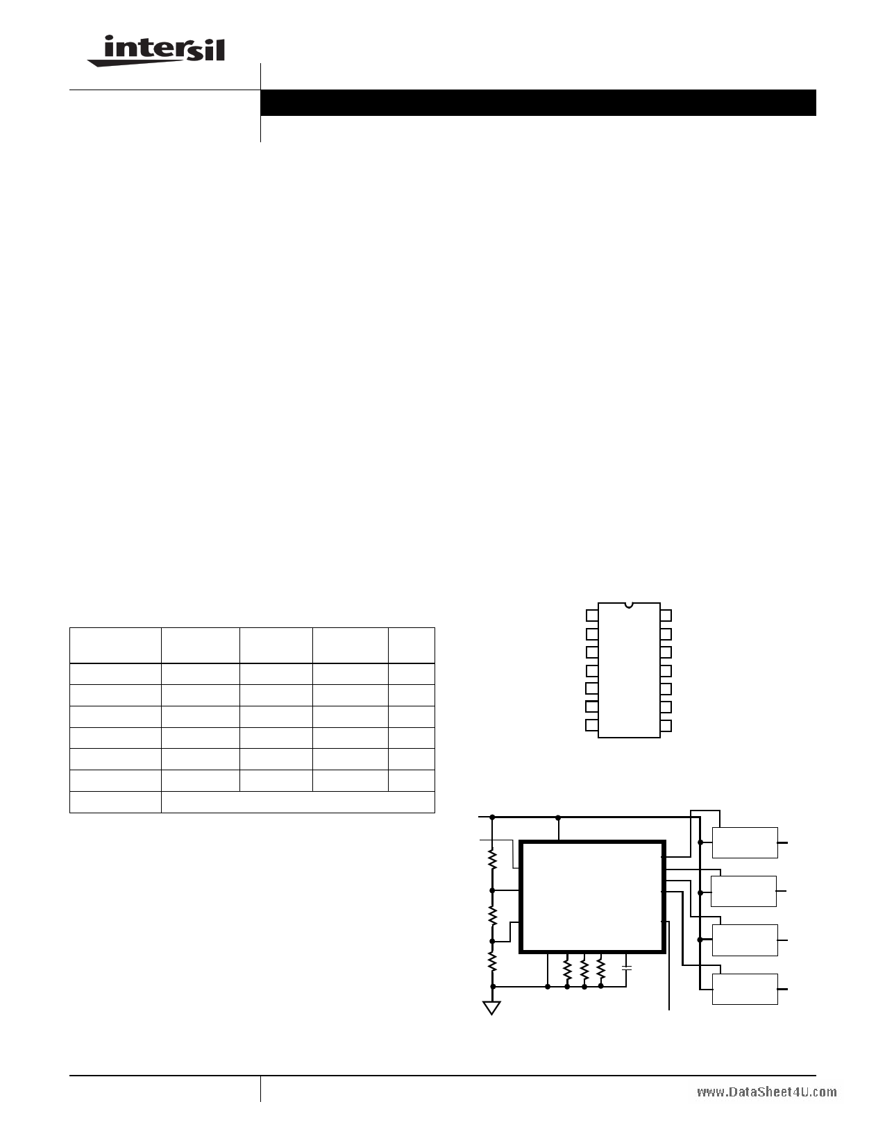
3.3-24V
Ru VIN ENABLE_A
SEQ_EN *
ENABLE_B
ENABLE_C
UV ENABLE_D
Rm
OV
FAULT *
GND TB TC TD TIME
Rl
EN
DC/DC
Vo1
EN
DC/DC
Vo2
EN
DC/DC
Vo3
EN
DC/DC
V04
* SEQ_EN and FAULT are not available on ISL8700A and ISL8701A
FIGURE 1. ISL870XA IMPLEMENTATION
1 CAUTION: These devices are sensitive to electrostatic discharge; follow proper IC Handling Procedures.
1-888-INTERSIL or 1-888-468-3774 | Intersil (and design) is a registered trademark of Intersil Americas Inc.
Copyright © Intersil Americas Inc. 2006. All Rights Reserved
All other trademarks mentioned are the property of their respective owners.
1 page 
ISL8700A, ISL8701A, ISL8702A, ISL8703A, ISL8704A, ISL8705A
On the ISL8702A, ISL8703A, ISL8704A and ISL8705A,
enabling of on or off sequencing can also be signaled via the
SEQ_EN or SEQ_EN# input pin once voltage compliance is
met. Initially, the SEQ_EN pin should be held low and
released when sequence start is desired. The SEQ# is
internally pulled high and sequencing is enabled when it is
pulled low. The on sequence of the ENABLE outputs is as
previously described. The off sequence feature is only
available on the variants having the SEQ_EN or the
SEQ_EN# inputs, these being the ISL8702A, ISL8703A,
ISL8704A, ISL8705A. The sequence is D off, then C off, then
B off and finally A off. Once SEQ_EN (SEQ_EN#) is signaled
low (high), the TIME cap is charged to 2V once again. Once
this Vth is reached, ENABLE_D transitions to its reset state
and CTIM is discharged. A delay and subsequent sequence
off is then determined by TD resistor to ENABLE_C. Likewise,
a delay to ENABLE_B and then ENABLE_A turn-off is
determined by TC and TB resistor values respectively.
With the ISL8700A, ISL8701A a quasi down sequencing of the
ENABLE outputs can be achieved by loading the ENABLE pins
with various value capacitors to ground. When a simultaneous
output latch off is invoked, the caps will set the falling ramp of
the various ENABLE outputs thus adjusting the time to Vth for
various DC/DC convertors or other circuitry.
Regardless of IC variant, the FAULT signal is always valid at
operational voltages and can be used as justification for
SEQ_EN release or even controlled with an RC timer for
sequence on.
Programming the Under and Overvoltage Limits
When choosing resistors for the divider remember to keep the
current through the string bounded by power loss at the top end
and noise immunity at the bottom end. For most applications,
total divider resistance in the 10kΩ to1000kΩ range is
advisable with high precision resistors being used to reduce
monitoring error. Although for the ISL870XA, two dividers of two
resistors each can be employed to separately monitor the OV
and UV levels for the VIN voltage. We will discuss using a
single three resistor string for monitoring the VIN voltage,
referencing Figure 1. In the three resistor divider string with Ru
(upper), Rm (middle) and Rl (lower), the ratios of each in
combination to the other two is balanced to achieve the desired
UV and OV trip levels. Although this IC has a bias range of 3.3V
to 24V, it can monitor any voltage >1.22V.
The ratio of the desired overvoltage trip point to the internal
reference is equal to the ratio of the two upper resistors to the
lowest (gnd connected) resistor.
The ratio of the desired undervoltage trip point to the internal
reference voltage is equal to the ratio of the uppermost (voltage
connected) resistor to the lower two resistors.
These assumptions are true for both rising (turn-on) or falling
(shutdown) voltages.
The following is a practical example worked out. For detailed
equatons on how to perform this operation for a given supply
requirement please see the next section.
1. Determine if turn-on or shutdown limits are preferred. In this
example, we will determine the resistor values based on the
shutdown limits.
2. Establish lower and upper trip level: 12V ±10% or 13.2V
(OV) and 10.8V (UV)
3. Establish total resistor string value: 100kΩ, Ir = divider
current
4. (Rm+Rl) x Ir = 1.1V @ UV and Rl x Ir = 1.2V @ OV
5. Rm+Rl = 1.1V/Ir @ UV = Rm+Rl = 1.1V/(10.8V/100kΩ) =
10.370kΩ
6. Rl = 1.2V/Ir @ OV = Rl = 1.2V/(13.2V/100kΩ) = 9.242kΩ
7. Rm = 10.370kΩ - 9.242kΩ = 1.128kΩ
8. Ru = 100kΩ - 10.370kΩ = 89.630kΩ
9. Choose standard value resistors that most closely
approximate these ideal values. Choosing a different total
divider resistance value may yield a more ideal ratio with
available resistor’s values.
In our example, with the closest standard values of
Ru = 90.9kΩ, Rm = 1.13kΩ and Rl = 9.31kΩ, the nominal UV
falling and OV rising will be at 10.9V and 13.3V respectively.
Programming the ENABLE Output Delays
The delay timing between the four sequenced ENABLE outputs
are programmed with four external passive components. The
delay from a valid VIN (ISL8700A and ISL8701A) to
ENABLE_A and SEQ_EN being valid (ISL8702A, ISL8703A,
ISL8704A, ISL8705A) to ENABLE_A is determined by the
value of the capacitor on the TIME pin to GND. The external
TIME pin capacitor is charged with a 2.6µA current source.
Once the voltage on TIME is charged up to the internal
reference voltage, (VTIME_VTH) the ENABLE_A output is
released out of its reset state. The capacitor value for a desired
delay (±10%) to ENABLE_A once VIN and SEQ_EN where
applicable has been satisfied is determined by:
CTIME = tVINSEQpd/770kΩ
Once ENABLE_A reaches VTIME_VTH, the TIME pin is pulled
low in preparation for a sequenced off signal via SEQ_EN. At
this time, the sequencing of the subsequent outputs is started.
ENABLE_B is released out of reset after a programmable time,
then ENABLE_C, then ENABLE _D, all with their own
programmed delay times.
The subsequent delay times are programmed with a single
external resistor for each ENABLE output providing maximum
flexibility to the designer through the choice of the resistor value
connected from TB, TC and TD pins to GND. The resistor
values determine the charge and discharge rate of an internal
capacitor comprising an RC time constant for an oscillator
whose output is fed into a counter generating the timing delay
to ENABLE output sequencing.
The RTX value for a given delay time is defined as:
RTX = tdel/1667nF
5 FN6381.0
October 12, 2006
5 Page 
ISL8700A, ISL8701A, ISL8702A, ISL8703A, ISL8704A, ISL8705A
.
PULL-UP
RESISTORS
TIMING
COMPONENTS
UV/OV SET
RESISTORS
FIGURE 16. ISL870XAEVAL1 PHOTOGRAPH AND SCHEMATIC OF LEFT CHANNEL
TABLE 1. ISL870XAEVAL1 LEFT CHANNEL COMPONENT LISTING
COMPONENT
DESIGNATOR
COMPONENT FUNCTION
COMPONENT DESCRIPTION
U1 ISL8702A, Quad Under/Overvoltage Sequencer
Intersil, ISL8702A, Quad Under/Overvoltage Sequencer
R3 UV Resistor for Divider String
1.1kΩ 1%, 0603
R2 VMONITOR Resistor for Divider String
88.7kΩ 1%, 0603
R5 OV Resistor for Divider String
9.1kΩ 1%, 0603
C1
R1
R9
R7
R4, R6, R8, R10,
R11
CTIME Sets Delay from Sequence Start to First ENABLE
RTD Sets Delay from Third to Fourth ENABLE
RTB Sets Delay from First to Second ENABLE
RTC Sets Delay from Second to Third ENABLE
ENABLE_X(#) and FAULT Pull-up Resistors
0.01μF, 0603
120kΩ 1%, 0603
3.01kΩ 1%, 0603
51kΩ 1%, 0603
4kΩ 10%, 0402
C3 Decoupling Capacitor
1μF, 0603
11 FN6381.0
October 12, 2006
11 Page | ||
| Páginas | Total 12 Páginas | |
| PDF Descargar | [ Datasheet ISL8703A.PDF ] | |
Hoja de datos destacado
| Número de pieza | Descripción | Fabricantes |
| ISL8703A | (ISL8700A - ISL8705A) Adjustable Quad Sequencer | Intersil Corporation |
| Número de pieza | Descripción | Fabricantes |
| SLA6805M | High Voltage 3 phase Motor Driver IC. |
Sanken |
| SDC1742 | 12- and 14-Bit Hybrid Synchro / Resolver-to-Digital Converters. |
Analog Devices |
|
DataSheet.es es una pagina web que funciona como un repositorio de manuales o hoja de datos de muchos de los productos más populares, |
| DataSheet.es | 2020 | Privacy Policy | Contacto | Buscar |