|
|
|
PDF ISL8105 Data sheet ( Hoja de datos )
| Número de pieza | ISL8105 | |
| Descripción | Single-Phase Synchronous Buck Converter PWM | |
| Fabricantes | Intersil Corporation | |
| Logotipo | ||
Hay una vista previa y un enlace de descarga de ISL8105 (archivo pdf) en la parte inferior de esta página. Total 17 Páginas | ||
|
No Preview Available !
®
Data Sheet
ISL8105, ISL8105A
December 6, 2006
FN6306.3
+5V or +12V Single-Phase Synchronous
Buck Converter PWM Controller with
Integrated MOSFET Gate Drivers
The ISL8105 is a simple single-phase PWM controller for a
synchronous buck converter. It operates from +5V or +12V bias
supply voltage. With integrated linear regulator, boot diode, and
N-channel MOSFET gate drivers, the ISL8105 reduces
external component count and board space requirements.
These make the IC suitable for a wide range of applications.
Utilizing voltage-mode control, the output voltage can be
precisely regulated to as low as 0.6V. The 0.6V internal
reference features a maximum tolerance of ±1.0% over the
commercial temperature range, and ±1.5% over the
industrial temperature range. Two fixed oscillator frequency
versions are available; 300kHz (ISL8105 for high efficiency
applications) and 600kHz (ISL8105A for fast transient
applications).
The ISL8105 features the capability of safe start-up with
pre-biased load. It also provides overcurrent protection by
monitoring the on resistance of the bottom-side MOSFET to
inhibit PWM operation appropriately. During start-up interval,
the resistor connected to BGATE/BSOC pin is employed to
program overcurrent protection condition. This approach
simplifies the implementation and does not deteriorate
converter efficiency.
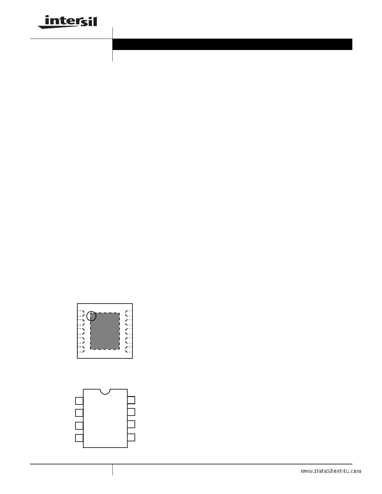
Pinouts
ISL8105
(10 LD 3X3 DFN)
TOP VIEW
BOOT 1
TGATE 2
N/C 3
GND 4
BGATE/BSOC 5
GND
10 LX
9 COMP/EN
8 FB
7 N/C
6 VBIAS
ISL8105
(8 LD SOIC)
TOP VIEW
BOOT 1
TGATE 2
GND 3
BGATE/BSOC 4
8 LX
7 COMP/EN
6 FB
5 VBIAS
Features
• Operates from +5V or +12V Bias Supply Voltage
- 1.0V to 12V Input Voltage Range (up to 20V possible
with restrictions; see Input Voltage Considerations)
- 0.6V to VIN Output Voltage Range
• 0.6V Internal Reference Voltage
- ±1.0% Tolerance Over the Commercial Temperature
Range (0°C to +70°C)
- ±1.5% Tolerance Over the Industrial Temperature
Range (-40°C to +85°C).
• Integrated MOSFET Gate Drivers that Operate from VBias
(+5V to +12V)
- Bootstrapped High-side Gate Driver with Integrated
Boot Diode
- Drives N-Channel MOSFETs
• Simple Voltage-Mode PWM Control
• Fast Transient Response
- High-Bandwidth Error Amplifier
- Full 0% to 100% Duty Cycle
• Fixed Operating Frequency
- 300kHz for ISL8105
- 600kHz for ISL8105A
• Fixed Internal Soft-Start with Pre-biased Load Capability
• Lossless, Programmable Overcurrent Protection
- Uses Bottom-side MOSFET’s rDS(ON)
• Enable/Disable Function Using COMP/EN Pin
• Output Current Sourcing and Sinking Currents
• Pb-Free Plus Anneal Available (RoHS Compliant)
Applications
• 5V or 12V DC/DC Regulators
• Industrial Power Systems
• Telecom and Datacom Applications
• Test and Measurement Instruments
• Distributed DC/DC Power Architecture
• Point of Load Modules
1 CAUTION: These devices are sensitive to electrostatic discharge; follow proper IC Handling Procedures.
1-888-INTERSIL or 1-888-468-3774 | Intersil (and design) is a registered trademark of Intersil Americas Inc.
Copyright Intersil Americas Inc. 2005-2006. All Rights Reserved
All other trademarks mentioned are the property of their respective owners.
1 page 
ISL8105, ISL8105A
Electrical Specifications Recommended Operating Conditions, Unless Otherwise Noted (Continued)
PARAMETER
SYMBOL
TEST CONDITIONS
MIN
TGATE Source Resistance
RTG-SRCl
TGATE Sink Resistance
RTG-SNKh
TGATE Sink Resistance
RTG-SNKl
BGATE Source Resistance
RBG-SRCh
BGATE Source Resistance
RBG-SRCl
BGATE Sink Resistance
RBG-SNKh
BGATE Sink Resistance
RBG-SNKl
OVERCURRENT PROTECTION (OCP)
VBias = 4.25V, 50mA Source Current
VBias = 14.5V, 50mA Source Current
VBias = 4.25V, 50mA Source Current
VBias = 14.5V, 50mA Source Current
VBias = 4.25V, 50mA Source Current
VBias = 14.5V, 50mA Source Current
VBias = 4.25V, 50mA Source Current
BSOC Current Source
IBSOC
ISL8105C; BGATE/BSOC Disabled
ISL8105I; BGATE/BSOC Disabled
19.5
18.0
TYP
3.5
2.7
2.7
2.4
2.75
2.0
2.1
21.5
21.5
MAX
UNITS
Ω
Ω
Ω
Ω
Ω
Ω
Ω
23.5 µA
23.5 µA
Functional Pin Description (SOIC, DFN)
BOOT (SOIC Pin 1, DFN Pin 1)
This pin provides ground referenced bias voltage to the
top-side MOSFET driver. A bootstrap circuit is used to create
a voltage suitable to drive an N-channel MOSFET (equal to
VBias minus the on-chip BOOT diode voltage drop), with
respect to LX.
TGATE (SOIC Pin 2, DFN Pin 2)
Connect this pin to the gate of top-side MOSFET; it provides
the PWM-controlled gate drive. It is also monitored by the
adaptive shoot-through protection circuitry to determine
when the top-side MOSFET has turned off.
GND (SOIC Pin 3, DFN Pin 4)
This pin represents the signal and power ground for the IC.
Tie this pin to the ground island/plane through the lowest
impedance connection available.
BGATE/BSOC (SOIC Pin 4, DFN Pin 5)
Connect this pin to the gate of the bottom-side MOSFET; it
provides the PWM-controlled gate drive (from VBias). This
pin is also monitored by the adaptive shoot-through
protection circuitry to determine when the lower MOSFET
has turned off.
During a short period of time following Power-On Reset
(POR) or shut-down release, this pin is also used to
determine the current limit threshold of the converter.
Connect a resistor (RBSOC) from this pin to GND. See
“Overcurrent Protection (OCP)” on page 7 for equations. An
overcurrent trip cycles the soft-start function, after two
dummy soft-start time-outs. Some of the text describing the
BGATE function may leave off the BSOC part of the name,
when it is not relevant to the discussion.
VBIAS (SOIC Pin 5, DFN Pin 6)
This pin provides the bias supply for the ISL8105, as well as
the bottom-side MOSFET's gate and the BOOT voltage for
the top-side MOSFET's gate. An internal 5V regulator will
supply bias if VBias rises above 6.5V (but the BGATE/BSOC
and BOOT will still be sourced by VBias). Connect a well
decoupled +5V or +12V supply to this pin.
FB (SOIC Pin 6, DFN Pin 8)
This pin is the inverting input of the internal error amplifier.
Use FB, in combination with the COMP/EN pin, to
compensate the voltage-control feedback loop of the
converter. A resistor divider from the output to GND is used
to set the regulation voltage.
COMP/EN (SOIC Pin 7, DFN Pin 9)
This is a multiplexed pin. During soft-start and normal converter
operation, this pin represents the output of the error amplifier.
Use COMP/EN, in combination with the FB pin, to compensate
the voltage-control feedback loop of the converter.
Pulling COMP/EN low (VDISABLE = 0.4V nominal) will
disable (shut-down) the controller, which causes the
oscillator to stop, the BGATE and TGATE outputs to be held
low, and the soft-start circuitry to re-arm. The external
pull-down device will initially need to overcome maximum of
5mA of COMP/EN output current. However, once the IC is
disabled, the COMP output will also be disabled, so only a
20µA current source will continue to draw current.
When the pull-down device is released, the COMP/EN pin
will start to rise at a rate determined by the 20µA charging up
the capacitance on the COMP/EN pin. When the COMP/EN
pin rises above the VDISABLE trip point, the ISL8105 will
begin a new initialization and soft-start cycle.
LX (SOIC Pin 8, DFN Pin 10)
Connect this pin to the source of the top-side MOSFET and
the drain of the bottom-side MOSFET. It is used as the sink
for the TGATE driver and to monitor the voltage drop across
the bottom-side MOSFET for overcurrent protection. This pin
is also monitored by the adaptive shoot-through protection
circuitry to determine when the top-side MOSFET has turned
off.
N/C (DFN Only; Pin3, Pin 7)
These two pins in the DFN package are No Connected.
5 FN6306.3
December 6, 2006
5 Page 
ISL8105, ISL8105A
BOOT
CBOOT
ISL8105
LX
+VBIAS
BGATE/BSOC
VBIAS
GND
GND
CVBIAS
+VIN
Q1 LO
Q2 CO
VOUT
C2
COMP
R2 C1
-
E/A +
FB
VREF
R3 C3
R1
FIGURE 8. PRINTED CIRCUIT BOARD SMALL SIGNAL
LAYOUT GUIDELINES
Figure 8 shows the circuit traces that require additional
layout consideration. Use single point and ground plane
construction for the circuits shown. Locate the resistor,
RBSOC, close to the BGATE/BSOC pin as the internal BSOC
current source is only 21.5µA. Minimize the loop from any
pulldown transistor connected to COMP/EN pin to reduce
antenna effect. Provide local decoupling between VBIAS
and GND pins as described earlier. Locate the capacitor,
CBOOT, as close as practical to the BOOT and LX pins. All
components used for feedback compensation (not shown)
should be located as close to the IC as practical.
Feedback Compensation
This section highlights the design considerations for a
voltage-mode controller requiring external compensation. To
address a broad range of applications, a type-3 feedback
network is recommended (see Figure 9).
Figure 9 highlights the voltage-mode control loop for a
synchronous-rectified buck converter, applicable to the
ISL805 circuit. The output voltage (VOUT) is regulated to the
reference voltage, VREF, level. The error amplifier output
(COMP pin voltage) is compared with the oscillator (OSC)
triangle wave to provide a pulse-width modulated wave with
an amplitude of VIN at the LX node. The PWM wave is
smoothed by the output filter (L and C). The output filter
capacitor bank’s equivalent series resistance is represented
by the series resistor ESR.
11
PWM
CIRCUIT
OSCILLATOR
VOSC
HALF-BRIDGE
DRIVE
VOUT
VIN
TGATE
LX
BGATE
L
DCR
C
ESR
ISL8105 EXTERNAL CIRCUIT
FIGURE 9. VOLTAGE-MODE BUCK CONVERTER
COMPENSATION DESIGN
The modulator transfer function is the small-signal transfer
function of VOUT/VCOMP. This function is dominated by a DC
gain, given by dMAXVIN/VOSC, and shaped by the output filter,
with a double pole break frequency at FLC and a zero at FCE.
For the purpose of this analysis, C and ESR represent the total
output capacitance and its equivalent series resistance.
FLC
=
-------------1--------------
2π ⋅ L ⋅ C
FCE = -2---π-----⋅---C----1--⋅---E----S-----R---
(EQ. 4)
The compensation network consists of the error amplifier
(internal to the ISL8105) and the external R1-R3, C1-C3
components. The goal of the compensation network is to
provide a closed loop transfer function with high 0dB crossing
frequency (F0; typically 0.1 to 0.3 of FSW) and adequate
phase margin (better than +45°). Phase margin is the
difference between the closed loop phase at F0dB and +180°.
The equations that follow relate the compensation network’s
poles, zeros and gain to the components (R1, R2, R3, C1, C2,
and C3) in Figure 9. Use the following guidelines for locating
the poles and zeros of the compensation network:
1. Select a value for R1 (1kΩ to 10kΩ, typically). Calculate
value for R2 for desired converter bandwidth (F0). If
setting the output voltage to be equal to the reference set
voltage as shown in Figure 9, the design procedure can
be followed as presented.
R2 = -d--V-M----O-A---S-X---C--⋅---V⋅---R-I--N--1---⋅-⋅--F-F---L-0--C---
(EQ. 5)
FN6306.3
December 6, 2006
11 Page | ||
| Páginas | Total 17 Páginas | |
| PDF Descargar | [ Datasheet ISL8105.PDF ] | |
Hoja de datos destacado
| Número de pieza | Descripción | Fabricantes |
| ISL8101 | Two-Phase Multiphase Buck PWM Controller | Intersil Corporation |
| ISL8102 | Two-Phase Buck PWM Controller | Intersil Corporation |
| ISL8103 | Three-Phase Buck PWM Controller | Intersil Corporation |
| ISL8104 | Synchronous Buck Pulse-Width Modulator (PWM) Controller | Intersil Corporation |
| Número de pieza | Descripción | Fabricantes |
| SLA6805M | High Voltage 3 phase Motor Driver IC. |
Sanken |
| SDC1742 | 12- and 14-Bit Hybrid Synchro / Resolver-to-Digital Converters. |
Analog Devices |
|
DataSheet.es es una pagina web que funciona como un repositorio de manuales o hoja de datos de muchos de los productos más populares, |
| DataSheet.es | 2020 | Privacy Policy | Contacto | Buscar |