|
|
PDF ISL6268 Data sheet ( Hoja de datos )
| Número de pieza | ISL6268 | |
| Descripción | High-Performance Notebook PWM Controller | |
| Fabricantes | Intersil Corporation | |
| Logotipo |  |
|
Hay una vista previa y un enlace de descarga de ISL6268 (archivo pdf) en la parte inferior de esta página. Total 14 Páginas | ||
|
No Preview Available !
®
Data Sheet
August 22, 2006
ISL6268
FN6348.0
High-Performance Notebook PWM
Controller
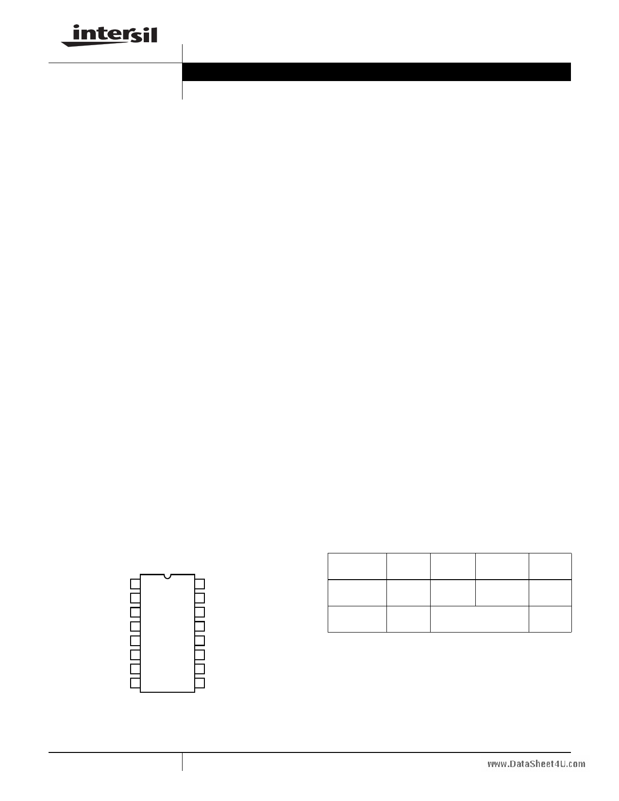
The ISL6268 IC is a Single-Phase Synchronous-Buck PWM
controller featuring Intersil's Robust Ripple Regulator (R3)
technology that delivers truly superior dynamic response to
input voltage and output load transients. Integrated
MOSFET drivers and bootstrap diode result in fewer
components and smaller implementation area.
Intersil’s R3 technology combines the best features of
fixed-frequency PWM and hysteretic PWM while eliminating
many of their shortcomings. R3 technology employs an
innovative modulator that synthesizes an AC ripple voltage
signal VR, analogous to the output inductor ripple current. The
AC signal VR enters a window comparator where the lower
threshold is the error amplifier output VCOMP, and the upper
threshold is a programmable voltage reference VW, resulting
in generation of the PWM signal. The voltage reference VW
sets the steady-state PWM frequency. Both edges of the
PWM can be modulated in response to input voltage
transients and output load transients, much faster than
conventional fixed-frequency PWM controllers. Unlike a
conventional hysteretic converter, the ISL6268 has an error
amplifier that provides ±1% voltage regulation at the FB pin.
The ISL6268 has a 1.5ms digital soft-start and can be
started into a pre-biased output voltage. A resistor divider is
used to program the output voltage setpoint. The ISL6268
normally operates in continuous-conduction-mode (CCM),
automatically entering diode-emulation-mode (DEM) at low
load for optimum efficiency. In CCM the converter operates
as a synchronous rectifier. In DEM the low-side MOSFET
stays off, blocking negative current flow from the output
inductor.
Pinout
ISL6268 (16 LD SSOP)
TOP VIEW
PHASE 1
PGOOD 2
VIN 3
VCC 4
EN 5
COMP 6
FB 7
GND 8
16 UG
15 BOOT
14 PVCC
13 LG
12 PGND
11 ISEN
10 VO
9 FSET
Features
• High performance R3 technology
• Fast transient response
• ±1% regulation accuracy: -10°C to +100°C
• Wide input voltage range: +7.0V to +25.0V
• Output voltage range: +0.6V to +3.3V
• Wide output load range: 0A to 25A
• Diode emulation mode for increased light load efficiency
• Programmable PWM frequency: 200kHz to 600kHz
• Pre-biased output start-up capability
• Integrated MOSFET drivers and bootstrap diode
• Internal digital soft-start
• Power good monitor
• Fault protection
- Undervoltage protection
- Soft crowbar overvoltage protection
- Low-side MOSFET r DS(on) overcurrent protection
- Over-temperature protection
- Fault identification by PGOOD pull-down resistance
• Pb-free plus anneal available (RoHS compliant)
Applications
• PCI express graphical processing unit
• Auxiliary power rail
• VRM
• Network adapter
Ordering Information
PART
PART
PKG.
NUMBER MARKING TEMP (°C) PACKAGE DWG. #
ISL6268CAZ 6268CAZ -10 to +100 16 Ld QSOP M16.15A
(Note)
(Pb-free)
ISL6268CAZ-T 6268CAZ 16 Ld QSOP Tape and
(Note)
Reel (Pb-free)
M16.15A
NOTE: Intersil Pb-free plus anneal products employ special Pb-free
material sets; molding compounds/die attach materials and 100%
matte tin plate termination finish, which are RoHS compliant and
compatible with both SnPb and Pb-free soldering operations. Intersil
Pb-free products are MSL classified at Pb-free peak reflow
temperatures that meet or exceed the Pb-free requirements of
IPC/JEDEC J STD-020.
1 CAUTION: These devices are sensitive to electrostatic discharge; follow proper IC Handling Procedures.
1-888-INTERSIL or 1-888-468-3774 | Intersil (and design) is a registered trademark of Intersil Americas Inc.
Copyright Intersil Americas Inc. 2006. All Rights Reserved
All other trademarks mentioned are the property of their respective owners.
1 page 
ISL6268
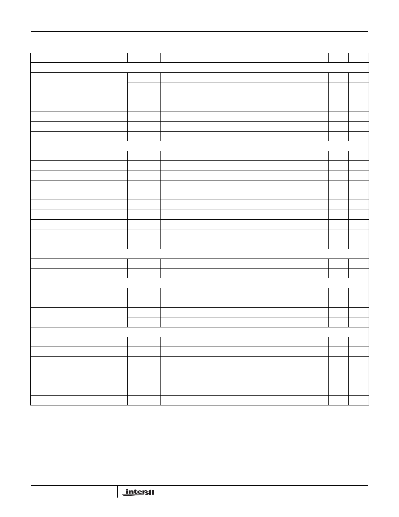
Electrical Specifications
PARAMETER
These specifications apply for TA = -10°C to +100°C, unless otherwise stated.
All typical specifications TA = +25°C, VCC = 5V, PVCC = 5V (Continued)
SYMBOL
TEST CONDITIONS
MIN
TYP MAX UNIT
POWER GOOD
PGOOD Pull-Down Impedance
PGOOD Leakage Current
PGOOD Maximum Sink Current (Note 2)
RPG_SS
RPG_UV
RPG_OV
RPG_OC
IPGOOD
PGOOD = 5mA Sink
PGOOD = 5mA Sink
PGOOD = 5mA Sink
PGOOD = 5mA Sink
PGOOD = 5V
75 95 125 Ω
75 95 125 Ω
50 63 85 Ω
25 32 45 Ω
- 0.1 1.0 µA
- 5.0 - mA
PGOOD Soft-Start Delay
GATE DRIVER
UG Pull-Up Resistance
UG Source Current (Note 2)
UG Sink Resistance
UG Sink Current (Note 2)
LG Pull-Up Resistance
LG Source Current (Note 2)
LG Sink Resistance
LG Sink Current (Note 2)
UG to LG Deadtime
LG to UG Deadtime
BOOTSTRAP DIODE
Forward Voltage
Reverse Leakage
CONTROL INPUTS
EN High Threshold
EN Low Threshold
EN Leakage
PROTECTION
TSS EN High to PGOOD High
RUGPU
IUGSRC
RUGPD
IUGSNK
RLGPU
ILGSRC
RLGPD
ILGSNK
tUGFLGR
tLGFUGR
200mA Source Current
UG - PHASE = 2.5V
250mA Sink Current
UG - PHASE = 2.5V
250mA Source Current
LG - PGND = 2.5V
250mA Sink Current
LG - PGND = 2.5V
UG falling to LG rising, no load
LG falling to UG rising, no load
VF PVCC = 5V, IF = 2mA
IR VR = 25V
VENTHR
VENTHF
IENL
IENH
EN = 0V
EN = 5.0V
2.20 2.75 3.30 ms
-
1.0 1.5
Ω
- 2.0 -
A
-
1.0 1.5
Ω
- 2.0 -
A
-
1.0 1.5
Ω
- 2.0 -
A
-
0.5 0.9
Ω
- 4.0 -
A
- 21 - ns
- 14 - ns
- 0.58 -
- 0.2 -
V
µA
2.0 -
-V
- - 1.0 V
- 0.1 1.0 µA
- 0.1 1.0 µA
ISEN OCP Threshold
ISEN Short-Circuit Threshold
UVP Threshold
OVP Rising Threshold
OVP Falling Threshold
OTP Rising Threshold (Note 2)
OTP Hysteresis (Note 2)
NOTE:
2. Guaranteed by characterization.
IOC
ISC
VUV
VOVR
VOVF
TOTR
TOTHYS
ISEN sourcing
ISEN sourcing
19 26 33
- 50 -
81 84 87
113 116 119
100 103 106
- 150 -
- 25 -
µA
µA
%
%
%
°C
°C
5 FN6348.0
August 22, 2006
5 Page 
ISL6268
General Application Design
This document is intended to provide a high-level explanation
of the steps necessary to create a single-phase power
converter. It is assumed that the reader is familiar with many
of the basic skills and techniques referenced in the following
sections. In addition to this document, Intersil provides
complete reference designs that include schematics, bills of
materials, and example board layouts.
Selecting the LC Output Filter
The duty cycle of an ideal buck converter is a function of the
input and the output voltage. This relationship is written as:
D = -V----O----U----T--
VIN
(EQ. 9)
The output inductor peak-to-peak ripple current is written as:
IPP
=
V-----O----U----T-----•--(---1-----–----D-----)
FSW • LOUT
(EQ. 10)
A typical step-down DC/DC converter will have an IPP of
20% to 40% of the maximum DC output load current. The
value of IPP is selected based upon several criteria such as
MOSFET switching loss, inductor core loss, and the resistive
loss of the inductor winding. The DC copper loss of the
inductor can be estimated by:
PCOPPER
=
IL
O
A
2
D
•
D
C
R
(EQ. 11)
where ILOAD is the converter output DC current.
The copper loss can be significant so attention has to be
given to the DCR selection. Another factor to consider when
choosing the inductor is its saturation characteristics at
elevated temperature. A saturated inductor could cause
destruction of circuit components, as well as nuisance OCP
faults.
A DC/DC buck regulator must have output capacitance
COUT into which ripple current IPP can flow. Current IPP
develops a corresponding ripple voltage VPP across COUT,
which is the sum of the voltage drop across the capacitor
ESR and of the voltage change stemming from charge
moved in and out of the capacitor. These two voltages are
written as:
∆VESR = IPP • ESR
(EQ. 12)
and
∆VC
=
----------------I--P----P-----------------
8 • COUT • FSW
(EQ. 13)
If the output of the converter has to support a load with high
pulsating current, several capacitors will need to be paralleled
to reduce the total ESR until the required VPP is achieved.
The inductance of the capacitor can cause a brief voltage dip
if the load transient has an extremely high slew rate. Low
inductance capacitors constructed with reverse package
geometry are available. A capacitor dissipates heat as a
function of RMS current and frequency. Be sure that IPP is
shared by a sufficient quantity of paralleled capacitors so that
they operate below the maximum rated RMS current at FSW.
Take into account that the rated value of a capacitor can fade
as much as 50% as the DC voltage across it increases.
Selection of the Input Capacitor
The important parameters for the bulk input capacitance are
the voltage rating and the RMS current rating. For reliable
operation, select bulk capacitors with voltage and current
ratings above the maximum input voltage and capable of
supplying the RMS current required by the switching circuit.
Their voltage rating should be at least 1.25 times greater
than the maximum input voltage, while a voltage rating of 1.5
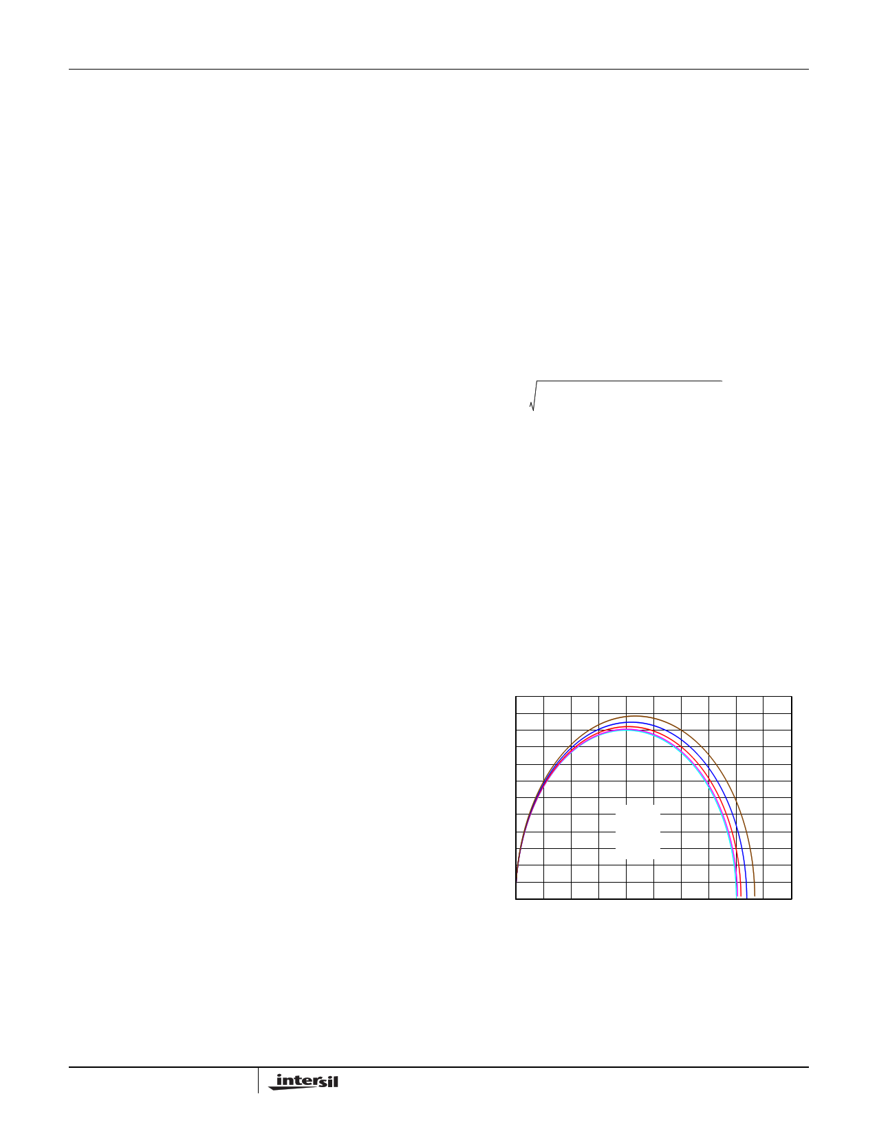
times is a preferred rating. Figure 6 is a graph of the input
RMS ripple current, normalized relative to output load current,
as a function of duty cycle that is adjusted for converter
efficiency. The ripple current calculation is written as:
IIN_RMS
=
(IM
A
2
X
⋅
(D
–
D2)
)
+
⎛
⎝
x
⋅
IMAX2
⋅1--D--2--
⎞
⎠
----------------------------------------------------------------------------------------------------
IMAX
(EQ. 14)
where:
- IMAX is the maximum continuous ILOAD of the converter
- x is a multiplier (0 to 1) corresponding to the inductor
peak-to-peak ripple amplitude expressed as a percentage
of IMAX (0% to 100%)
- D is the duty cycle that is adjusted to take into account the
efficiency of the converter which is written as:
D = ------V----O-----U----T-------
VIN ⋅ EFF
(EQ. 15)
In addition to the bulk capacitance, some low ESL ceramic
capacitance is recommended to decouple between the drain
of the high-side MOSFET and the source of the low-side
MOSFET.
0.6
0.55
0.5
0.45
0.4
0.35
0.3
0.25
0.2
0.15
0.1
0.05
0
0
x=1
x = 0.75
x = 0.50
x = 0.25
x=0
0.1 0.2 0.3 0.4 0.5 0.6 0.7 0.8 0.9
DUTY CYCLE
1
FIGURE 6. NORMALIZED RMS INPUT CURRENT FOR x = 0.8
11 FN6348.0
August 22, 2006
11 Page | ||
| Páginas | Total 14 Páginas | |
| PDF Descargar | [ Datasheet ISL6268.PDF ] | |
Hoja de datos destacado
| Número de pieza | Descripción | Fabricantes |
| ISL6260 | Multi-Phase Core Regulator | Intersil Corporation |
| ISL6260B | Multi-Phase Core Regulator | Intersil Corporation |
| ISL6260C | Multiphase PWM Regulator | Intersil Corporation |
| ISL6261 | Single Phase Core Regulator | Intersil |
| Número de pieza | Descripción | Fabricantes |
| SLA6805M | High Voltage 3 phase Motor Driver IC. |
Sanken |
| SDC1742 | 12- and 14-Bit Hybrid Synchro / Resolver-to-Digital Converters. |
Analog Devices |
|
DataSheet.es es una pagina web que funciona como un repositorio de manuales o hoja de datos de muchos de los productos más populares, |
| DataSheet.es | 2020 | Privacy Policy | Contacto | Buscar |
