|
|
|
PDF ISL83083E Data sheet ( Hoja de datos )
| Número de pieza | ISL83083E | |
| Descripción | (ISL83080E - ISL83088E) RS-485/RS-422 Transceivers | |
| Fabricantes | Intersil Corporation | |
| Logotipo | ||
Hay una vista previa y un enlace de descarga de ISL83083E (archivo pdf) en la parte inferior de esta página. Total 18 Páginas | ||
|
No Preview Available !
®
Data Sheet
ISL83080E, ISL83082E, ISL83083E,
ISL83085E, ISL83086E, ISL83088E
September 12, 2005
FN6085.6
±15kV ESD Protected, 5V, Full Fail-Safe,
Fractional (1/8) Unit Load, RS-485/RS-422
Transceivers
The ISL8308XE are BiCMOS, ESD protected, 5V powered,
single transceivers that meet both the RS-485 and RS-422
standards for balanced communication. Each driver output,
and receiver input, is protected against ±15kV ESD strikes
without latch-up, and unlike competitive products, this Intersil
family is specified for 10% tolerance supplies (4.5V to 5.5V).
These devices have very low bus currents (+125µA/-75µA),
so they present a true “1/8 unit load” to the RS-485 bus. This
allows up to 256 transceivers on the network without violating
the RS-485 specification’s 32 unit load maximum, and without
using repeaters. For example, in a remote utility meter reading
system, individual meter readings are routed to a concentrator
via an RS-485 network, so the high allowed node count
minimizes the number of repeaters required. Data for all
meters is then read out from the concentrator via a single
access port, or a wireless link.
Receiver (Rx) inputs feature a “Full Fail-Safe” design, which
ensures a logic high Rx output if Rx inputs are floating,
shorted, or terminated but undriven.
www.DataSheet4U.com
The ISL83080E, ISL83082E, ISL83083E, ISL83085E utilize
slew rate limited drivers which reduce EMI, and minimize
reflections from improperly terminated transmission lines, or
unterminated stubs in multidrop and multipoint applications.
Slew rate limited versions also include receiver input filtering to
enhance noise immunity in the presence of slow input signals.
Hot Plug circuitry ensures that the Tx and Rx outputs remain
in a high impedance state until the power supply has
stabilized, and the Tx outputs are fully short circuit protected.
The ISL83080E, ISL83083E, ISL83086E are configured for
full duplex (separate Rx input and Tx output pins)
applications. The half duplex versions multiplex the Rx inputs
and Tx outputs to allow transceivers with output disable
functions in 8 lead packages.
Features
• Pb-Free Plus Anneal Available (RoHS Compliant)
(See Ordering Info)
• RS-485 I/O Pin ESD Protection . . . . . . . . . . ±15kV HBM
Class 3 ESD Protection (HBM) on all Pins. . . . . . . . >7kV
• Full Fail-safe (Open, Short, Terminated and Floating)
Receivers
• Hot Plug Circuitry (ISL83080E, ISL83082E, ISL83083E,
ISL83085E)
- Tx and Rx Outputs Remain Three-state During Power-
up/Power-down
• True 1/8 Unit Load Allows up to 256 Devices on the Bus
• Specified for Single 5V, 10% Tolerance, Supplies
• High Data Rates. . . . . . . . . . . . . . . . . . . . . up to 10Mbps
• Low Quiescent Supply Current . . . . . . . . . . . . . . . 530µA
Ultra Low Shutdown Supply Current . . . . . . . . . . . . 70nA
• -7V to +12V Common Mode Input Voltage Range
• Half and Full Duplex Pinouts
• Three-State Rx and Tx Outputs
• Current Limiting and Thermal Shutdown for driver
Overload Protection
Applications
• Automated Utility Meter Reading Systems
• High Node Count Systems
• Factory Automation
• Field Bus Networks
• Security Camera Networks
• Building Environmental Control Systems
• Industrial/Process Control Networks
PART
NUMBER
ISL83080E
ISL83082E
ISL83083E
ISL83085E
ISL83086E
ISL83088E
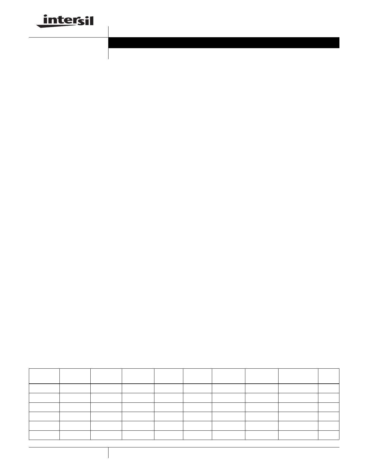
TABLE 1. SUMMARY OF FEATURES
HALF/FULL DATA RATE SLEW-RATE
# DEVICES
Rx/Tx
DUPLEX
(Mbps)
LIMITED? HOT PLUG ON BUS ENABLE?
Full 0.115 Yes
Yes 256
Yes
Half 0.115
Yes
Yes 256
Yes
Full 0.5 Yes Yes 256 Yes
Half 0.5
Yes Yes 256 Yes
Full 10
No
No 256
Yes
Half 10
No
No 256
Yes
QUIESCENT
ICC (µA)
530
530
530
530
530
530
LOW POWER PIN
SHUTDOWN? COUNT
Yes 14
Yes 8
Yes 14
Yes 8
Yes 14
Yes 8
1 CAUTION: These devices are sensitive to electrostatic discharge; follow proper IC Handling Procedures.
1-888-INTERSIL or 321-724-7143 | Intersil (and design) is a registered trademark of Intersil Americas Inc.
Copyright © Intersil Americas Inc. 2004-2005. All Rights Reserved
All other trademarks mentioned are the property of their respective owners.
1 page 
ISL83080E, ISL83082E, ISL83083E, ISL83085E, ISL83086E, ISL83088E
Absolute Maximum Ratings
VCC to Ground. . . . . . . . . . . . . . . . . . . . . . . . . . . . . . . . . . . . . . . 7V
Input Voltages
DI, DE, RE . . . . . . . . . . . . . . . . . . . . . . . . . -0.3V to (VCC + 0.3V)
Input/Output Voltages
A, B, Y, Z . . . . . . . . . . . . . . . . . . . . . . . . . . . . . . . . . . -9V to +13V
A, B, Y, Z (Transient Pulse Through 100Ω) . . . . . . . . . . . . . ±25V
RO . . . . . . . . . . . . . . . . . . . . . . . . . . . . . . . . -0.3V to (VCC +0.3V)
Short Circuit Duration
Y, Z . . . . . . . . . . . . . . . . . . . . . . . . . . . . . . . . . . . . . . . Continuous
ESD Rating . . . . . . . . . . . . . . . . . . . . . . . . . See Specification Table
Thermal Information
Thermal Resistance (Typical, Note 3)
θJA (°C/W)
8 Ld SOIC Package . . . . . . . . . . . . . . . . . . . . . . . . .
105
8 Ld MSOP Package . . . . . . . . . . . . . . . . . . . . . . . .
140
14 Ld SOIC Package . . . . . . . . . . . . . . . . . . . . . . . .
128
Maximum Junction Temperature (Plastic Package) . . . . . . . 150°C
Maximum Storage Temperature Range . . . . . . . . . . . -65°C to 150°C
Maximum Lead Temperature (Soldering 10s) . . . . . . . . . . . . 300°C
(Lead Tips Only)
Operating Conditions
Temperature Range . . . . . . . . . . . . . . . . . . . . . . . . . . . -40°C to 85°C
CAUTION: Stresses above those listed in “Absolute Maximum Ratings” may cause permanent damage to the device. This is a stress only rating and operation of the
device at these or any other conditions above those indicated in the operational sections of this specification is not implied.
NOTE:
3. θJA is measured with the component mounted on a high effective thermal conductivity test board in free air. See Tech Brief TB379 for details.
Electrical Specifications Test Conditions: VCC = 4.5V to 5.5V; Unless Otherwise Specified. Typicals are at VCC = 5V, TA = 25°C
(Note 4)
PARAMETER
SYMBOL
TEST CONDITIONS
TEMP
(°C) MIN
TYP MAX UNITS
DC CHARACTERISTICS
Driver Differential VOUT (no load)
Driver Differential VOUT (with load)
Change in Magnitude of Driver
Differential VOUT for
Complementary Output States
VOD1
VOD2
∆VOD
RL = 100Ω (RS-422) (Figure 1A)
RL = 54Ω (RS-485) (Figure 1A)
RL = 60Ω, -7V ≤ VCM ≤ 12V (Figure 1B)
RL = 54Ω or 100Ω (Figure 1A)
Full -
Full 2
Full 1.5
Full 1.5
Full -
-
2.9
2.4
2.6
0.01
VCC
-
VCC
-
0.2
V
V
V
V
V
Driver Common-Mode VOUT
Change in Magnitude of Driver
Common-Mode VOUT for
Complementary Output States
VOC
∆VOC
RL = 54Ω or 100Ω (Figure 1A)
RL = 54Ω or 100Ω (Figure 1A)
Full - 2.85 3
V
Full - 0.01 0.1 V
Logic Input High Voltage
Logic Input Low Voltage
DI Input Hysteresis Voltage
Logic Input Current
Input Current (A, B)
Output Leakage Current (Y, Z)
(Full Duplex Versions Only)
Output Leakage Current (Y, Z)
in Shutdown Mode (Full Duplex)
Driver Short-Circuit Current,
VO = High or Low
Receiver Differential Threshold
Voltage
VIH
VIL
VHYS
IIN1
IIN2
IIN3
IIN3
IOSD1
DE, DI, RE
DE, DI, RE
DE, DI, RE
DE = 0V, VCC = 0V or 5.5V VIN = 12V
VIN = -7V
RE = 0V, DE = 0V, VCC = 0V VIN = 12V
or 5.5V
VIN = -7V
RE = VCC, DE = 0V, VCC = 0V VIN = 12V
or 5.5V
VIN = -7V
DE = VCC, -7V ≤ VY or VZ ≤ 12V (Note 6)
VTH -7V ≤ VCM ≤ 12V
Full 2
Full -
25 -
Full -2
Full -
Full -75
Full -
Full -75
Full -
Full -20
Full -
- -V
- 0.8 V
100 - mV
- 2 µA
70 125 µA
55 - µA
7 125 µA
11 - µA
0 20 µA
9 - µA
- ±250 mA
Full -200 -90
-50 mV
Receiver Input Hysteresis
∆VTH VCM = 0V
25 - 20 - mV
5 FN6085.6
September 12, 2005
5 Page 
ISL83080E, ISL83082E, ISL83083E, ISL83085E, ISL83086E, ISL83088E
Receivers easily meet the data rates supported by the
corresponding driver, and all receiver outputs are three-
statable via the active low RE input.
Driver Features
The RS-485/422 driver is a differential output device that
delivers at least 1.5V across a 54Ω load (RS-485), and at
least 2V across a 100Ω load (RS-422). The drivers feature
low propagation delay skew to maximize bit width, and to
minimize EMI.
All drivers are three-statable via the active high DE input.
The 115kbps and 500kbps driver outputs are slew rate
limited to minimize EMI, and to minimize reflections in
unterminated or improperly terminated networks. Outputs of
the ISL83086E, ISL83088E drivers are not limited, so faster
output transition times allow data rates of at least 10Mbps.
Hot Plug Function
When a piece of equipment powers up, there is a period of
time where the processor or ASIC driving the RS-485 control
lines (DE, RE) is unable to ensure that the RS-485 Tx and
Rx outputs are kept disabled. If the equipment is connected
to the bus, a driver activating prematurely during power up
may crash the bus. To avoid this scenario, the ISL83080,
ISL83082, ISL83083, ISL83085 versions incorporate a “Hot
Plug” function. Circuitry monitoring VCC ensures that, during
power up and power down, the Tx and Rx outputs remain
disabled, regardless of the state of DE and RE, if VCC is less
than ~3.4V. This gives the processor/ASIC a chance to stabilize
and drive the RS-485 control lines to the proper states.
VCC
5
A/Y
2.5
0
RO
3.4V
3.2V
DI = VCC
5
2.5
0
ISL83080E
RL = 1kΩ
ISL83080E
5
RL = 1kΩ
2.5
0
TIME (40µs/DIV)
FIGURE 7. HOT PLUG PERFORMANCE (ISL83080E) vs
DEVICE WITHOUT HOT PLUG CIRCUITRY
(ISL83086E)
ESD Protection
All pins on these devices include class 3 Human Body
Model (HBM) ESD protection structures, but the RS-485
pins (driver outputs and receiver inputs) incorporate
advanced structures allowing them to survive ESD events
in excess of ±15kV HBM. The RS-485 pins are particularly
vulnerable to ESD damage because they typically connect
11
to an exposed port on the exterior of the finished product.
Simply touching the port pins, or connecting a cable, can
cause an ESD event that might destroy unprotected ICs.
These new ESD structures protect the device whether or
not it is powered up, protect without allowing any latchup
mechanism to activate, and without degrading the RS-485
common mode range of -7V to +12V. This built-in ESD
protection eliminates the need for board level protection
structures (e.g., transient suppression diodes), and the
associated, undesirable capacitive load they present.
Data Rate, Cables, and Terminations
RS-485/422 are intended for network lengths up to 4000’,
but the maximum system data rate decreases as the
transmission length increases. Devices operating at 10Mbps
are limited to lengths less than 100’, while the 115kbps
versions can operate at full data rates with lengths of several
thousand feet.
Twisted pair is the cable of choice for RS-485/422 networks.
Twisted pair cables tend to pick up noise and other
electromagnetically induced voltages as common mode
signals, which are effectively rejected by the differential
receivers in these ICs.
Proper termination is imperative, when using the 10Mbps
devices, to minimize reflections. Short networks using the
115kbps versions need not be terminated, but, terminations
are recommended unless power dissipation is an overriding
concern.
In point-to-point, or point-to-multipoint (single driver on bus)
networks, the main cable should be terminated in its
characteristic impedance (typically 120Ω) at the end farthest
from the driver. In multi-receiver applications, stubs
connecting receivers to the main cable should be kept as
short as possible. Multipoint (multi-driver) systems require
that the main cable be terminated in its characteristic
impedance at both ends. Stubs connecting a transceiver to
the main cable should be kept as short as possible.
Built-In Driver Overload Protection
As stated previously, the RS-485 spec requires that drivers
survive worst case bus contentions undamaged. These
devices meet this requirement via driver output short circuit
current limits, and on-chip thermal shutdown circuitry.
The driver output stages incorporate short circuit current
limiting circuitry which ensures that the output current never
exceeds the RS-485 spec, even at the common mode
voltage range extremes. Additionally, these devices utilize a
foldback circuit which reduces the short circuit current, and
thus the power dissipation, whenever the contending voltage
exceeds either supply.
In the event of a major short circuit condition, devices also
include a thermal shutdown feature that disables the drivers
whenever the die temperature becomes excessive. This
eliminates the power dissipation, allowing the die to cool. The
drivers automatically re-enable after the die temperature
drops about 15 degrees. If the contention persists, the thermal
shutdown/re-enable cycle repeats until the fault is cleared.
Receivers stay operational during thermal shutdown.
FN6085.6
September 12, 2005
11 Page | ||
| Páginas | Total 18 Páginas | |
| PDF Descargar | [ Datasheet ISL83083E.PDF ] | |
Hoja de datos destacado
| Número de pieza | Descripción | Fabricantes |
| ISL83083E | (ISL83080E - ISL83088E) RS-485/RS-422 Transceivers | Intersil Corporation |
| Número de pieza | Descripción | Fabricantes |
| SLA6805M | High Voltage 3 phase Motor Driver IC. |
Sanken |
| SDC1742 | 12- and 14-Bit Hybrid Synchro / Resolver-to-Digital Converters. |
Analog Devices |
|
DataSheet.es es una pagina web que funciona como un repositorio de manuales o hoja de datos de muchos de los productos más populares, |
| DataSheet.es | 2020 | Privacy Policy | Contacto | Buscar |