|
|
|
PDF 40REC0770-QB Data sheet ( Hoja de datos )
| Número de pieza | 40REC0770-QB | |
| Descripción | GaAs Receiver QFN | |
| Fabricantes | Mimix Broadband | |
| Logotipo | ||
Hay una vista previa y un enlace de descarga de 40REC0770-QB (archivo pdf) en la parte inferior de esta página. Total 7 Páginas | ||
|
No Preview Available !
35.0-45.0 GHz GaAs Receiver
QFN, 7x7 mm
October 2006 - Rev 05-Oct-06
Features
Sub-harmonic Receiver
Integrated LNA, Image Reject Mixer, LO Doubler/Buffer
+2.0 dBm LO Drive Level
8.0 dB Conversion Gain
4.0 dB NF
+5.0 dBm Input Third Order Intercept (IP3)
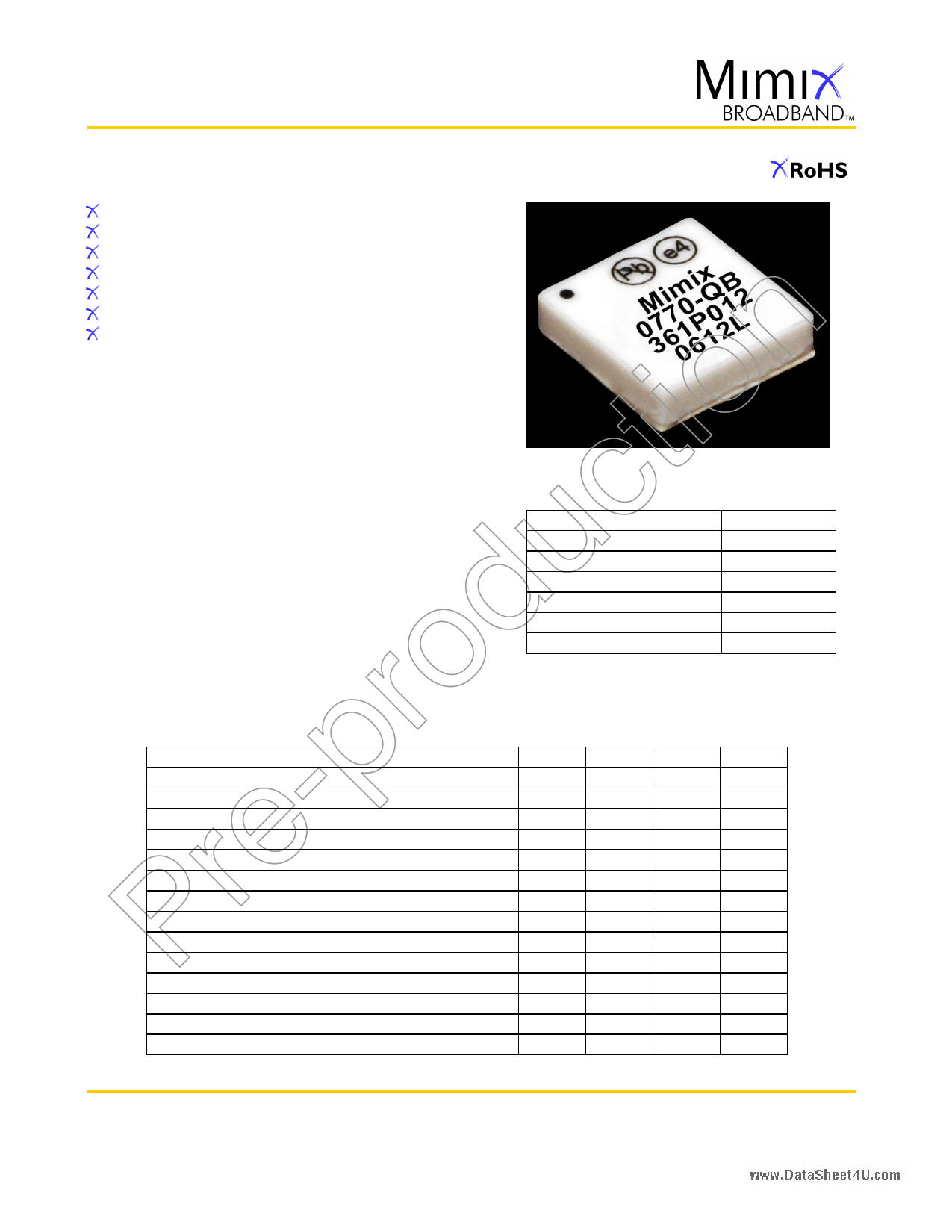
7x7mm QFN package
40REC0770-QB
General Description
Mimix Broadband’s 35.0-45.0 GHz packaged receiver has a
noise figure of 4.0 dB and 5.0 dBm Input Third Order
Intercept across the band.This device integrates a three
stage LNA followed by an image reject resistive pHEMT
mixer and includes an integrated LO doubler and buffer
amplifier.The use of integrated LO doubler and LO buffer
amplifier makes the provision of the LO easier than for
fundamental mixers at these frequencies. I and Q mixer
outputs are provided and an external 90 degree hybrid is
required to select the desired sideband. The device comes
in a 7x7mm QFN package that is RoHS compliant. This
device is well suited for Millimeter-wave Point-to-Point
Radio, LMDS, SATCOM and VSAT applications.
Absolute Maximum Ratings
Supply Voltage (Vd)
Supply Current (Id)
Gate Bias Voltage (Vg)
Input Power (RF Pin)
Storage Temperature (Tstg)
Operating Temperature (Ta)
Channel Temperature (Tch)
+6.0 VDC
300 mA
+0.3 VDC
+5 dBm
-65 to +165 OC
-55 to MTTF Table1
MTTF Table1
(1) Channel temperature affects a device's MTTF. It is
recommended to keep channel temperature as low as
possible for maximum life.
Electrical Characteristics (Ambient Temperature T = 25o C)
Parameter
Units Min. Typ. Max.
Frequency Range (RF)
GHz 35.0 - 45.0
Frequency Range (LO)
GHz 16.0 - 24.0
Frequency Range (IF)
GHz DC - 4.0
Input Return Loss RF (S11)
dB - 10.0 -
Small Signal Conversion Gain RF/IF (S21)
dB - 8.0 -
LO Input Drive (PLO)
dBm - +2.0 -
Image Rejection
dBc - 20.0 -
Noise Figure (NF)
dB - 4.0 -
Isolation LO/RF @ LOx1/LOx2
dB - 40.0/40.0 -
Input Third Order Intercept (IIP3)
dBm - +5.0 -
Input 1 dB Compression (IP1dB)
dBm - -5.0 -
Drain Bias Voltage (Vd)
VDC - +4.0 +5.5
Gate Bias Voltage (Vg1,2)
VDC -1.2 -0.5 +0.1
Supply Current (Id) (Vd=4.0, Vg=-0.3V Typical)
mA - 180 240
Mimix Broadband, Inc., 10795 Rockley Rd., Houston, Texas 77099
Tel: 281.988.4600 Fax: 281.988.4615 mimixbroadband.com
Page 1 of 7
Characteristic Data and Specifications are subject to change without notice. ©2006 Mimix Broadband, Inc.
Export of this item may require appropriate export licensing from the U.S. Government. In purchasing these parts, U.S. Domestic customers accept
their obligation to be compliant with U.S. Export Laws.
1 page 
35.0-45.0 GHz GaAs Receiver
QFN, 7x7 mm
October 2006 - Rev 05-Oct-06
40REC0770-QB
App Note [1] Biasing - The device is operated by biasing VD=4.0V with ID=180 mA. Additionally, a mixer and doubler bias are also required
with VG2=-0.5V. Adjusting Vg2 above or below this value can adversely affect conversion gain, image rejection and intercept point
performance. It is recommended to use active biasing to keep the currents constant as the RF power and temperature vary; this gives the
most reproducible results. Depending on the supply voltage available and the power dissipation constraints, the bias circuit may be a single
transistor or a low power operational amplifier, with a low value resistor in series with the drain supply used to sense the current.The gate of
the pHEMT is controlled to maintain correct drain current and thus drain voltage.The typical gate voltage needed to do this is -0.3V.Typically
the gate is protected with Silicon diodes to limit the applied voltage. Also, make sure to sequence the applied voltage to ensure negative
gate bias is available before applying the positive drain supply.
MTTF
MTTF is calculated from accelerated life-time data of single devices and assumes an isothermal back-plate.
1.E+05
40REC0770-QB, MTTF (yrs) vs. Backplate Temperature (°C)
1.E+04
1.E+03
1.E+02
1.E+01
1.E+00
55
Typical Application
RF IN
37.0-39.5 GHz
65 75 85
Temperature (°C)
Bias Conditions: Vd=4.0V, Id=180 mA
40REC0770-QB
Coupler
95
BPF
IF Out
2 GHz
LNA IR Mixer
Buffer
AGC Control
X2
LO(+2.0dBm)
17.5-18.75 GHz (USB Operation)
19.5-20.75 GHz (LSB Operation)
Mimix Broadband MMIC-based 35.0-45.0 GHz Receiver Block Diagram
(Changing LO and IF frequencies as required allows design to operate as high as 46 GHz)
Mimix Broadband's 30.0-46.0 GHz 40REC0770-QB GaAs MMIC Receiver can be used in saturated radio applications and linear modulation
schemes up to 128 QAM.
Mimix Broadband, Inc., 10795 Rockley Rd., Houston, Texas 77099
Tel: 281.988.4600 Fax: 281.988.4615 mimixbroadband.com
Page 5 of 7
Characteristic Data and Specifications are subject to change without notice. ©2006 Mimix Broadband, Inc.
Export of this item may require appropriate export licensing from the U.S. Government. In purchasing these parts, U.S. Domestic customers accept
their obligation to be compliant with U.S. Export Laws.
5 Page | ||
| Páginas | Total 7 Páginas | |
| PDF Descargar | [ Datasheet 40REC0770-QB.PDF ] | |
Hoja de datos destacado
| Número de pieza | Descripción | Fabricantes |
| 40REC0770-QB | GaAs Receiver QFN | Mimix Broadband |
| Número de pieza | Descripción | Fabricantes |
| SLA6805M | High Voltage 3 phase Motor Driver IC. |
Sanken |
| SDC1742 | 12- and 14-Bit Hybrid Synchro / Resolver-to-Digital Converters. |
Analog Devices |
|
DataSheet.es es una pagina web que funciona como un repositorio de manuales o hoja de datos de muchos de los productos más populares, |
| DataSheet.es | 2020 | Privacy Policy | Contacto | Buscar |