|
|
|
PDF HI5760 Data sheet ( Hoja de datos )
| Número de pieza | HI5760 | |
| Descripción | A/D Converter | |
| Fabricantes | Intersil Corporation | |
| Logotipo | ||
Hay una vista previa y un enlace de descarga de HI5760 (archivo pdf) en la parte inferior de esta página. Total 18 Páginas | ||
|
No Preview Available !
®
Data Sheet
March 30, 2005
HI5760
FN4320.8
10-Bit, 125/60MSPS, High Speed D/A
Converter
The HI5760 is a 10-bit, 125MSPS, high speed, low power,
D/A converter which is implemented in an advanced CMOS
process. Operating from a single +3V to +5V supply, the
converter provides 20mA of full scale output current and
includes edge-triggered CMOS input data latches. Low glitch
energy and excellent frequency domain performance are
achieved using a segmented current source architecture.
For an equivalent performance dual version, see the HI5728.
This device complements the HI5X60 family of high speed
converters offered by Intersil, which includes 8, 10, 12, and
14-bit devices.
Ordering Information
PART
TEMP.
PKG. CLOCK
NUMBER RANGE (oC) PACKAGE NO. SPEED
HI5760BIB
-40 to 85 28 Ld SOIC M28.3 125MHz
HI5760BIBZ
(See Note)
-40 to 85 28 Ld SOIC M28.3 125MHz
(Pb-free)
HI5760IA
www.DataSheet4U.comHI5760IAZ
(See Note)
-40 to 85
-40 to 85
28 Ld TSSOP M28.173 125MHz
28 Ld TSSOP M28.173 125MHz
(Pb-free)
HI5760/6IB
-40 to 85 28 Ld SOIC M28.3 60MHz
HI5760/6IBZ
(See Note)
-40 to 85 28 Ld SOIC M28.3 60MHz
(Pb-free)
HI5760EVAL1
25 Evaluation Platform 125MHz
* Add “-T” suffix for tape and reel.
NOTE: Intersil Pb-free products employ special Pb-free material
sets; molding compounds/die attach materials and 100% matte tin
plate termination finish, which are RoHS compliant and compatible
with both SnPb and Pb-free soldering operations. Intersil Pb-free
products are MSL classified at Pb-free peak reflow temperatures that
meet or exceed the Pb-free requirements of IPC/JEDEC J STD-020.
Features
• Throughput Rate . . . . . . . . . . . . . . . . . . . . . . . . 125MSPS
• Low Power . . . . . . . . . . . . . . . 165mW at 5V, 27mW at 3V
• Power Down Mode. . . . . . . . . . 23mW at 5V, 10mW at 3V
• Integral Linearity Error . . . . . . . . . . . . . . . . . . . . . . ±1 LSB
• Adjustable Full Scale Output Current. . . . . 2mA to 20mA
• SFDR to Nyquist at 5MHz Output . . . . . . . . . . . . . . 68dBc
• Internal 1.2V Temperature Compensated Bandgap
Voltage Reference
• Single Power Supply from +5V to +3V
• CMOS Compatible Inputs
• Excellent Spurious Free Dynamic Range
• Pb-Free Available (RoHS Compliant)
Applications
• Cable Modems
• Set Top Boxes
• Wireless Communications
• Direct Digital Frequency Synthesis
• Signal Reconstruction
• Test Instrumentation
• High Resolution Imaging Systems
• Arbitrary Waveform Generators
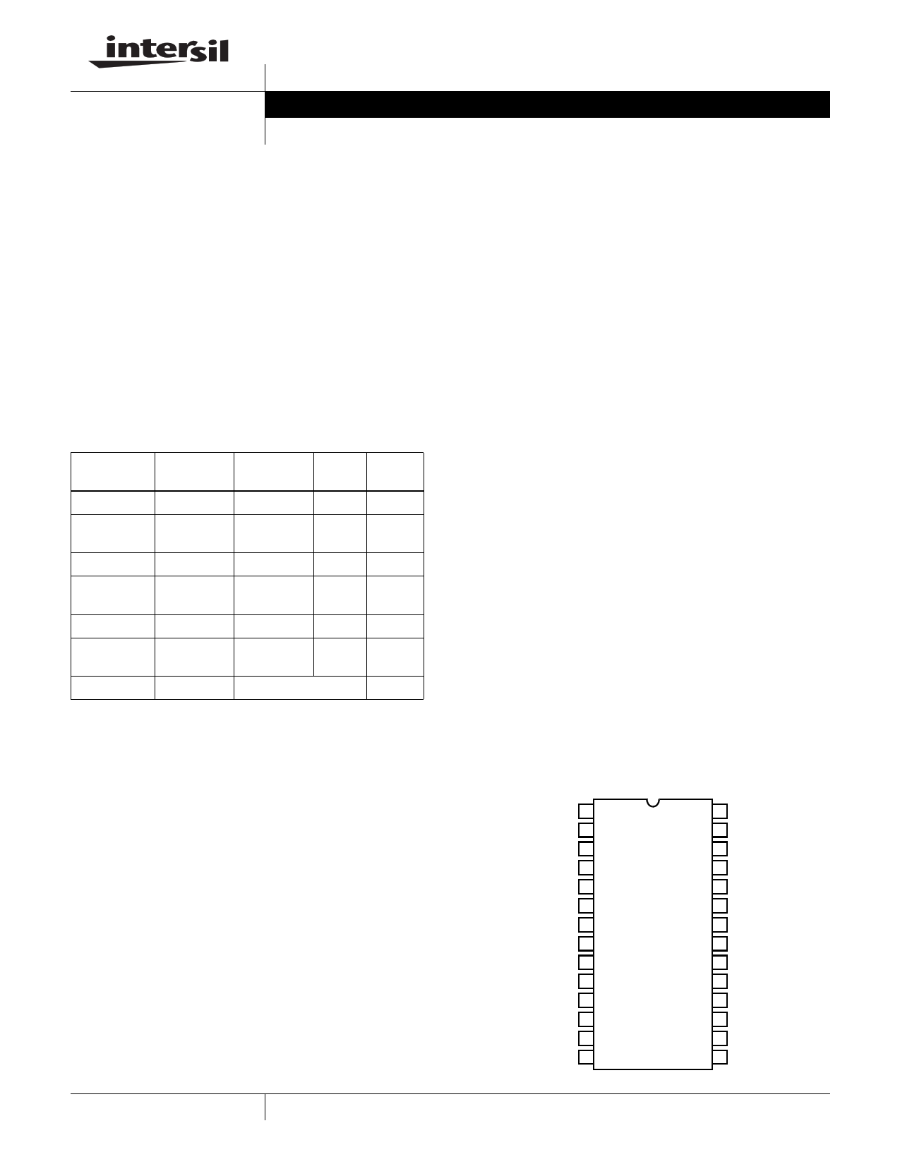
Pinout
HI5760 (SOIC, TSSOP)
TOP VIEW
D9 (MSB) 1
D8 2
D7 3
D6 4
D5 5
D4 6
D3 7
D2 8
D1 9
D0 (LSB) 10
NC 11
NC 12
NC 13
NC 14
28 CLK
27 DVDD
26 DCOM
25 NC
24 AVDD
23 NC
22 IOUTA
21 IOUTB
20 ACOM
19 COMP1
18 FSADJ
17 REFIO
16 REFLO
15 SLEEP
1 CAUTION: These devices are sensitive to electrostatic discharge; follow proper IC Handling Procedures.
1-888-INTERSIL or 321-724-7143 | Intersil (and design) is a registered trademark of Intersil Americas Inc.
Copyright © Intersil Americas Inc. 2003, 2005. All Rights Reserved
All other trademarks mentioned are the property of their respective owners.
1 page 
HI5760
Electrical Specifications AVDD = DVDD = +5V, VREF = Internal 1.2V, IOUTFS = 20mA, TA = 25oC for All Typical Values (Continued)
PARAMETER
TEST CONDITIONS
HI5760
TA = -40oC TO 85oC
MIN TYP MAX
UNITS
DIGITAL INPUTS D9-D0, CLK
Input Logic High Voltage with
5V Supply, VIH
Input Logic High Voltage with
3V Supply, VIH
Input Logic Low Voltage with
5V Supply, VIL
Input Logic Low Voltage with
3V Supply, VIL
Input Logic Current, IIH
Input Logic Current, IIL
Digital Input Capacitance, CIN
TIMING CHARACTERISTICS
(Note 3)
(Note 3)
(Note 3)
(Note 3)
3.5 5
-
V
2.1 3
-
V
- 0 1.3 V
- 0 0.9 V
-10 - +10 µA
-10 - +10 µA
- 5 - pF
Data Setup Time, tSU
See Figure 41 (Note 3)
Data Hold Time, tHLD
See Figure 41 (Note 3)
Propagation Delay Time, tPD
See Figure 41
CLK Pulse Width, tPW1, tPW2
See Figure 41 (Note 3)
POWER SUPPLY CHARACTERISTICS
3 - - ns
3 - - ns
- 1 - ns
4 - - ns
AVDD Power Supply
DVDD Power Supply
Analog Supply Current (IAVDD)
(Note 8)
(Note 8)
(5V or 3V, IOUTFS = 20mA)
(5V or 3V, IOUTFS = 2mA)
2.7 5.0 5.5
2.7 5.0 5.5
- 23 30
-4-
V
V
mA
mA
Digital Supply Current (IDVDD)
(5V, IOUTFS = Don’t Care) (Note 5)
(3V, IOUTFS = Don’t Care) (Note 5)
- 35
- 1.5 -
mA
mA
Supply Current (IAVDD) Sleep Mode
Power Dissipation
(5V or 3V, IOUTFS = Don’t Care)
(5V, IOUTFS = 20mA) (Note 6)
- 1.6 3
- 165 -
mA
mW
(5V, IOUTFS = 2mA) (Note 6)
- 70 - mW
(5V, IOUTFS = 20mA) (Note 9)
- 150 -
mW
(3.3V, IOUTFS = 20mA) (Note 9)
- 75 - mW
(3V, IOUTFS = 20mA) (Note 6)
- 85 - mW
(3V, IOUTFS = 20mA) (Note 9)
- 67 - mW
(3V, IOUTFS = 2mA) (Note 6)
- 27 - mW
Power Supply Rejection
Single Supply (Note 7)
-0.2 - +0.2 % FSR/V
NOTES:
2. Gain Error measured as the error in the ratio between the full scale output current and the current through RSET (typically 625µA). Ideally the
ratio should be 31.969.
3. Parameter guaranteed by design or characterization and not production tested.
4. Spectral measurements made with differential coupled transformer.
5. Measured with the clock at 50MSPS and the output frequency at 1MHz.
6. Measured with the clock at 100MSPS and the output frequency at 40MHz.
7. See ‘Definition of Specifications’.
8. It is recommended that the output current be reduced to 12mA or less to maintain optimum performance for operation below 3V. DVDD and AVDD
do not have to be equal.
9. Measured with the clock at 60MSPS and the output frequency at 10MHz.
5
5 Page 
HI5760
Typical Performance Curves, 3V Power Supply (Continued)
80
75
70
65
60
55
50
45
40
-40
-20
2.5MHz
10.1MHz
40.4MHz
0 20 40
TEMPERATURE (oC)
60
80
FIGURE 30. SFDR vs TEMPERATURE, CLOCK = 100MSPS
-10
-20
-30
-40
-50
-60
-70
-80
-90
-100
-110
0
fCLK = 100MSPS
fOUT = 9.95MHz
AMPLITUDE = 0dBFS
SFDR = 63dBc
14dB EXTERNAL
ANALYZER ATTENUATION
5MHz/DIV.
FREQUENCY (MHz)
FIGURE 31. SINGLE TONE SFDR
50
-20
-30
-40
-50
-60
-70
-80
-90
-100
-110
0
fCLK = 100MSPS
fOUT = 13.5/14.5MHz
COMBINED PEAK
AMPLITUDE = 0dBFS
SFDR = 61.5dBc
14dB EXTERNAL
ANALYZER ATTENUATION
5MHz / DIV.
FREQUENCY (MHz)
50
FIGURE 32. TWO-TONE, CLOCK = 100MSPS
-10
-20
-30
-40
-50
-60
-70
-80
-90
-100
0.5
fCLK = 100MSPS
fOUT = 3.8,4.4,5.6,6.2MHz
COMBINED PEAK
AMPLITUDE = 0dBFS
SFDR = 70.6dBc
(IN A WINDOW)
1.45MHz / DIV.
FREQUENCY (MHz)
15
FIGURE 33. FOUR-TONE, CLOCK = 100MSPS
-20
-30
-40
-50
-60
-70
-80
-90
-100
-110
0.5
fCLK = 100MSPS
fOUT = 2.6, 3.2, 3.8, 4.4,
5.6, 6.2, 6.8MHz
COMBINED PEAK
AMPLITUDE = 0dBFS
SFDR = 67.4dBc
(IN A WINDOW)
1.95MHz / DIV.
FREQUENCY (MHz)
20
FIGURE 34. EIGHT-TONE, CLOCK = 100MSPS
11
-10
-20
-30
-40
-50
-60
-70
-80
-90
-100
0
fCLK = 50MSPS
fOUT = 1.9, 2.2, 2.8, 3.1MHz
COMBINED PEAK
AMPLITUDE = 0dBFS
SFDR = 74.2dBc
(IN A WINDOW)
950kHz / DIV.
FREQUENCY (MHz)
10
FIGURE 35. FOUR-TONE, CLOCK = 50MSPS
11 Page | ||
| Páginas | Total 18 Páginas | |
| PDF Descargar | [ Datasheet HI5760.PDF ] | |
Hoja de datos destacado
| Número de pieza | Descripción | Fabricantes |
| HI5760 | A/D Converter | Intersil Corporation |
| HI5762 | A/D Converter | Intersil Corporation |
| HI5766 | A/D Converter | Intersil Corporation |
| HI5767 | A/D Converter | Intersil Corporation |
| Número de pieza | Descripción | Fabricantes |
| SLA6805M | High Voltage 3 phase Motor Driver IC. |
Sanken |
| SDC1742 | 12- and 14-Bit Hybrid Synchro / Resolver-to-Digital Converters. |
Analog Devices |
|
DataSheet.es es una pagina web que funciona como un repositorio de manuales o hoja de datos de muchos de los productos más populares, |
| DataSheet.es | 2020 | Privacy Policy | Contacto | Buscar |