|
|
|
PDF HI5731 Data sheet ( Hoja de datos )
| Número de pieza | HI5731 | |
| Descripción | A/D Converter | |
| Fabricantes | Intersil Corporation | |
| Logotipo | ||
Hay una vista previa y un enlace de descarga de HI5731 (archivo pdf) en la parte inferior de esta página. Total 17 Páginas | ||
|
No Preview Available !
®
Data Sheet
September 15, 2004
HI5731
FN4070.9
12-Bit, 100MSPS, High Speed D/A
Converter
The HI5731 is a 12-bit, 100MSPS, D/A converter which is
implemented in the Intersil BiCMOS 10V (HBC-10) process.
Operating from +5V and -5.2V, the converter provides
-20.48mA of full scale output current and includes an input
data register and bandgap voltage reference. Low glitch
energy and excellent frequency domain performance are
achieved using a segmented architecture. The digital inputs
are TTL/CMOS compatible and translated internally to ECL.
All internal logic is implemented in ECL to achieve high
switching speed with low noise. The addition of laser
trimming assures 12-bit linearity is maintained along the
entire transfer curve.
Ordering Information
TEMP.
PART NUMBER RANGE (°C)
PKG. DWG.
PACKAGE
#
HI5731BIP
-40 to 85 28 Ld PDIP
E28.6
HI5731BIPZ
(See Note)
-40 to 85 28 Ld PDIP
(Pb-free)
E28.6
HI5731BIB
www.DataSheet4U.com
HI5731BIB-T
-40 to 85 28 Ld SOIC
28 Ld SOIC Tape and Reel
M28.3
M28.3
HI5731BIBZ
(See Note)
-40 to 85 28 Ld SOIC
(Pb-free)
M28.3
HI5731-EVS
25 Evaluation Board (SOIC)
NOTE: Intersil Pb-free products employ special Pb-free material
sets; molding compounds/die attach materials and 100% matte tin
plate termination finish, which is compatible with both SnPb and
Pb-free soldering operations. Intersil Pb-free products are MSL
classified at Pb-free peak reflow temperatures that meet or exceed
the Pb-free requirements of IPC/JEDEC J STD-020C.
Features
• Pb-free Available as an Option
• Throughput Rate . . . . . . . . . . . . . . . . . . . . . . . . 100MSPS
• Low Power . . . . . . . . . . . . . . . . . . . . . . . . . . . . . . .650mW
• Integral Linearity Error . . . . . . . . . . . . . . . . . . . . 0.75 LSB
• Low Glitch Energy . . . . . . . . . . . . . . . . . . . . . . . . . 3.0pV-s
• TTL/CMOS Compatible Inputs
• Improved Hold Time . . . . . . . . . . . . . . . . . . . . . . . . 0.25ns
• Excellent Spurious Free Dynamic Range
Applications
• Cellular Base Stations
• GSM Base Stations
• Wireless Communications
• Direct Digital Frequency Synthesis
• Signal Reconstruction
• Test Equipment
• High Resolution Imaging Systems
• Arbitrary Waveform Generators
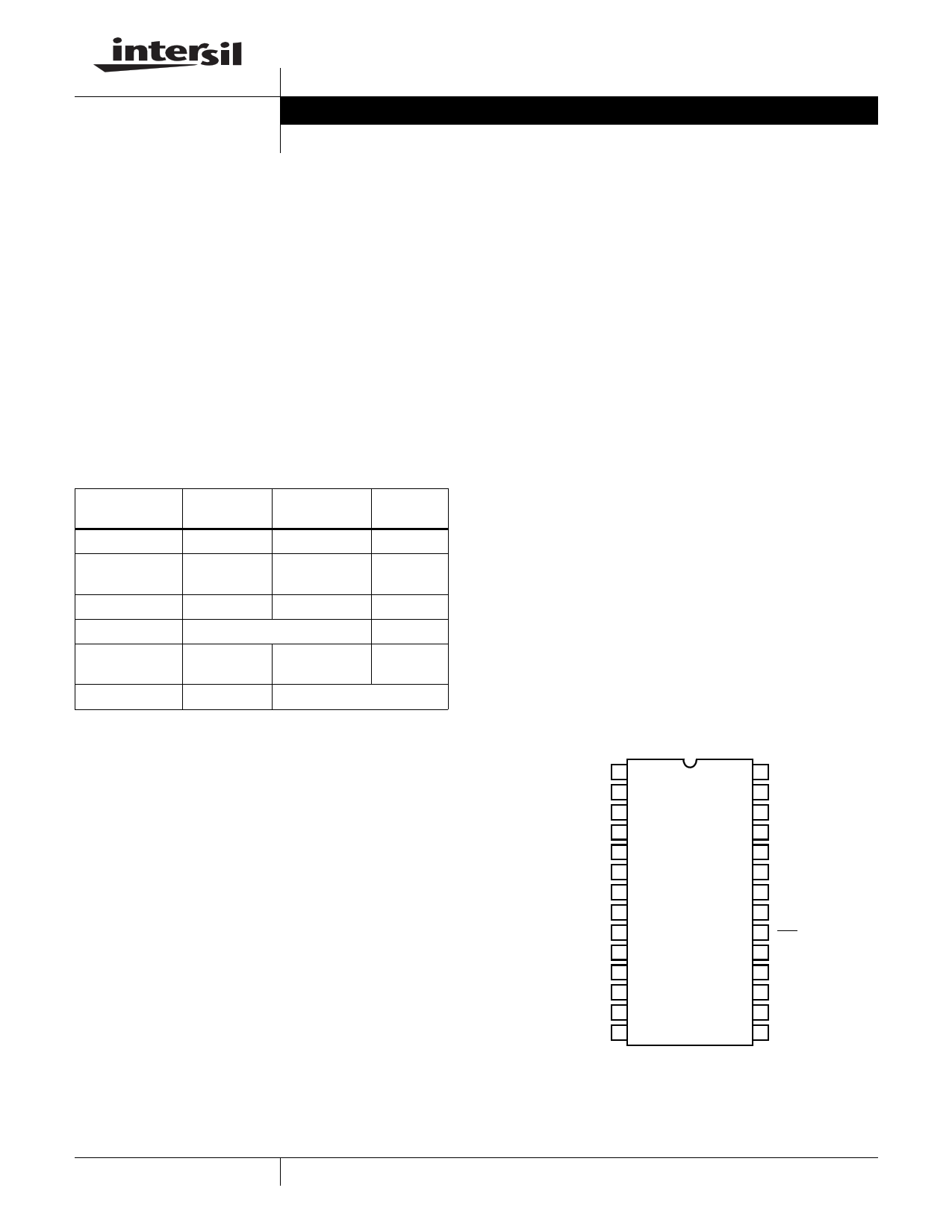
Pinout
HI5731
(PDIP, SOIC)
TOP VIEW
D11 (MSB) 1
D10 2
D9 3
D8 4
D7 5
D6 6
D5 7
D4 8
D3 9
D2 10
D1 11
D0 (LSB) 12
NC 13
NC 14
28 DGND
27 AGND
26 REF OUT
25 CTRL OUT
24 CTRL IN
23 RSET
22 AVEE
21 IOUT
20 IOUT
19 ARTN
18 DVEE
17 DGND
16 DVCC
15 CLOCK
1 CAUTION: These devices are sensitive to electrostatic discharge; follow proper IC Handling Procedures.
1-888-INTERSIL or 321-724-7143 | Intersil (and design) is a registered trademark of Intersil Americas Inc.
Copyright © Intersil Americas Inc. 2002, 2004. All Rights Reserved
1 page 
Timing Diagrams
HI5731
CLK
50%
D11-D0
IOUT
±1/2 LSB ERROR BAND
tSETT
tPD
FIGURE 1. FULL SCALE SETTLING TIME DIAGRAM
V GLITCH AREA = 1/2 (H x W)
HEIGHT (H)
WIDTH (W)
t (ps)
FIGURE 2. PEAK GLITCH AREA (SINGLET) MEASUREMENT
METHOD
CLK
D11-D0
IOUT
tPW1
tPW2
tSU tSU tSU
tHLD
tHLD
tHLD
50%
tPD
tPD tPD
FIGURE 3. PROPAGATION DELAY, SETUP TIME, HOLD TIME AND MINIMUM PULSE WIDTH DIAGRAM
5
5 Page 
HI5731
be chosen so that the effective output resistance (ROUT)
matches the line resistance. The output voltage is:
VOUT = IOUT x ROUT.
IOUT is defined in the reference section. IOUT is not trimmed
to 12 bits, so it is not recommended that it be used in
conjunction with IOUT in a differential-to-single-ended
application. The compliance range of the output is from -
1.25V to 0V, with a 1VP-P voltage swing allowed within this
range.
TABLE 2. INPUT CODING vs CURRENT OUTPUT
INPUT CODE (D11-D0)
1111 1111 1111
IOUT (mA)
-20.48
IOUT (mA)
0
1000 0000 0000
-10.24
-10.24
0000 0000 0000
0 -20.48
as glitch when changing the DAC output. Units are typically
specified in picoVolt-seconds (pV-s).
HI5731
(21) IOUT
100MHz SCOPE
LOW PASS
FILTER
64Ω 50Ω
FIGURE 25. GLITCH TEST CIRCUIT
Settling Time
The settling time of the HI5731 is measured as the time it
takes for the output of the DAC to settle to within a ±1/2 LSB
error band of its final value during a full scale (code 0000...
to 1111.... or 1111... to 0000...) transition. All claims made by
Intersil with respect to the settling time performance of the
HI5731 have been fully verified by the National Institute of
Standards and Technology (NIST) and are fully traceable.
Glitch
The output glitch of the HI5731 is measured by summing the
area under the switching transients after an update of the
DAC. Glitch is caused by the time skew between bits of the
incoming digital data. Typically, the switching time of digital
inputs are asymmetrical meaning that the turn off time is
faster than the turn on time (TTL designs). Unequal delay
paths through the device can also cause one current source
to change before another. In order to minimize this, the
Intersil HI5731 employes an internal register, just prior to the
current sources, which is updated on the clock edge. Lastly,
the worst case glitch on traditional D/A converters usually
occurs at the major transition (i.e., code 2047 to 2048).
However, due to the split architecture of the HI5731, the
glitch is moved to the 255 to 256 transition (and every
subsequent 256 code transitions thereafter). This split R/2R
segmented current source architecture, which decreases the
amount of current switching at any one time, makes the
glitch practically constant over the entire output range. By
making the glitch a constant size over the entire output range
this effectively integrates this error out of the end application.
In measuring the output glitch of the HI5731 the output is
terminated into a 64Ω load. The glitch is measured at any
one of the current cell carry (code 255 to 256 transition or
any multiple thereof) throughout the DACs output range.
The glitch energy is calculated by measuring the area under
the voltage-time curve. Figure 26 shows the area considered
a (mV)
t (ns)
GLITCH ENERGY = (a x t)/2
FIGURE 26. MEASURING GLITCH ENERGY
Applications
Bipolar Applications
To convert the output of the HI5731 to a bipolar 4V swing,
the following applications circuit is recommended. The
reference can only provide 125µA of drive, so it must be
buffered to create the bipolar offset current needed to
generate the -2V output with all bits ‘off’. The output current
must be converted to a voltage and then gained up and
offset to produce the proper swing. Care must be taken to
compensate for the voltage swing and error.
REF OUT
(26)
-
+
1/2 CA2904
5kΩ
HI5731
IOUT
(21)
50Ω
5kΩ
-
+
1/2 CA2904
60Ω
0.1µF
240Ω
240Ω
- VOUT
+
HFA1100
FIGURE 27. BIPOLAR OUTPUT CONFIGURATION
11
11 Page | ||
| Páginas | Total 17 Páginas | |
| PDF Descargar | [ Datasheet HI5731.PDF ] | |
Hoja de datos destacado
| Número de pieza | Descripción | Fabricantes |
| HI5731 | A/D Converter | Intersil Corporation |
| HI5735 | A/D Converter | Intersil Corporation |
| Número de pieza | Descripción | Fabricantes |
| SLA6805M | High Voltage 3 phase Motor Driver IC. |
Sanken |
| SDC1742 | 12- and 14-Bit Hybrid Synchro / Resolver-to-Digital Converters. |
Analog Devices |
|
DataSheet.es es una pagina web que funciona como un repositorio de manuales o hoja de datos de muchos de los productos más populares, |
| DataSheet.es | 2020 | Privacy Policy | Contacto | Buscar |