|
|
|
PDF UMA6NT1 Data sheet ( Hoja de datos )
| Número de pieza | UMA6NT1 | |
| Descripción | (UMA4NT1 / UMA6NT1) Dual Common Emitter Bias Resistor Transistors | |
| Fabricantes | ON Semiconductor | |
| Logotipo | ||
Hay una vista previa y un enlace de descarga de UMA6NT1 (archivo pdf) en la parte inferior de esta página. Total 5 Páginas | ||
|
No Preview Available !
UMA4NT1, UMA6NT1
Preferred Devices
Dual Common Emitter Bias
Resistor Transistors
PNP Silicon Surface Mount Transistors
with Monolithic Bias Resistor Network
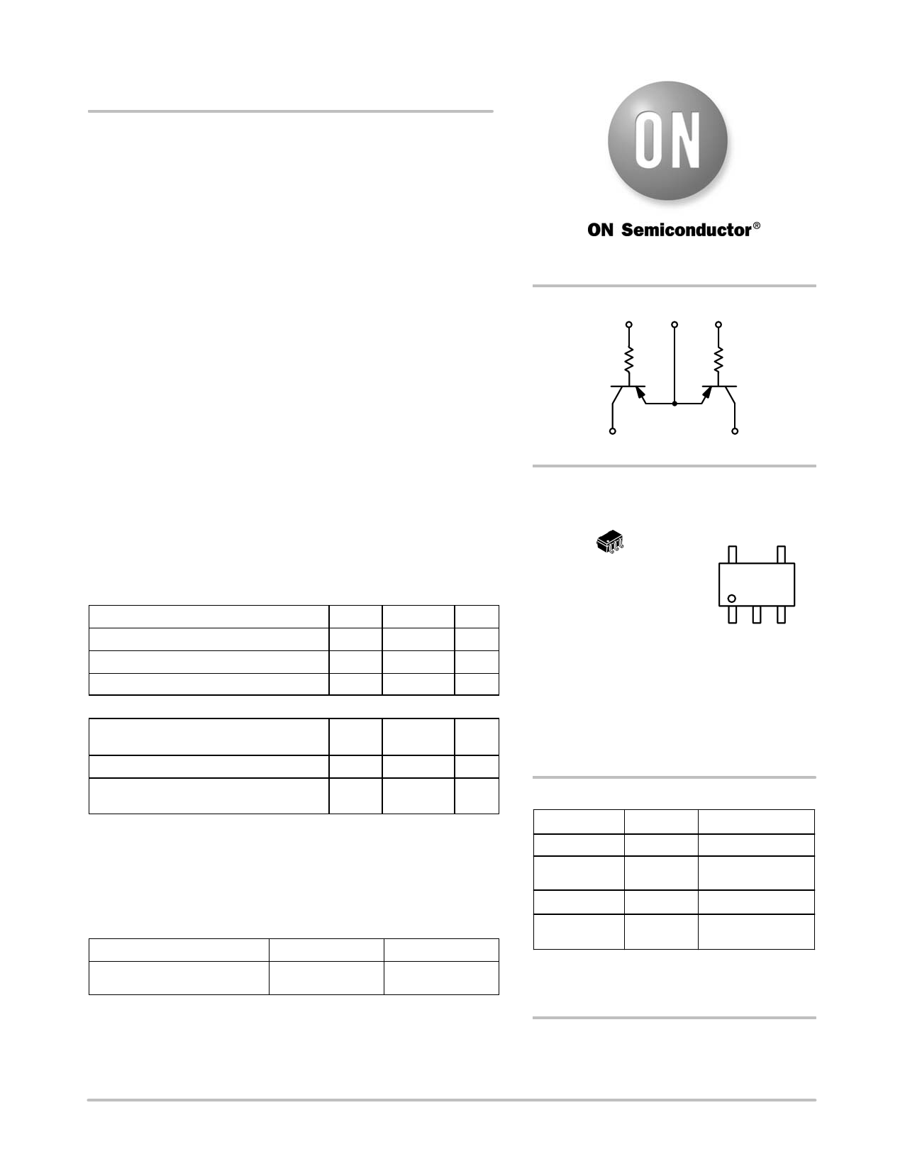
The BRT (Bias Resistor Transistor) contains a single transistor with
a monolithic bias network consisting of two resistors; a series base
resistor and a base−emitter resistor. These digital transistors are
designed to replace a single device and its external resistor bias
network. The BRT eliminates these individual components by
integrating them into a single device. In the UMC2NT1 series, two
BRT devices are housed in the SOT−353 package which is ideal for
low power surface mount applications where board space is at a
premium.
Features
• Simplifies Circuit Design
• Reduces Board Space
• Reduces Component Count
• Pb−Free Packages are Available
MAXIMUM RATINGS (TA = 25°C unless otherwise noted, cwowmw.mDaotanShefoetr4UQ.co1m
and Q2, − minus sign for Q1 (PNP) omitted)
Rating
Symbol Value
Unit
Collector-Base Voltage
Collector-Emitter Voltage
Collector Current
THERMAL CHARACTERISTICS
VCBO
VCEO
IC
50 Vdc
50 Vdc
100 mAdc
Thermal Resistance, Junction-to-Ambient
(Surface Mounted)
RqJA
833 °C/W
Operating and Storage Temperature Range
Total Package Dissipation @ TA = 25°C
(Note 1)
TJ, Tstg
PD
−65 to +150
*150
°C
mW
Stresses exceeding Maximum Ratings may damage the device. Maximum
Ratings are stress ratings only. Functional operation above the Recommended
Operating Conditions is not implied. Extended exposure to stresses above the
Recommended Operating Conditions may affect device reliability.
1. Device mounted on a FR-4 glass epoxy printed circuit board using the
minimum recommended footprint.
DEVICE RESISTOR VALUES
Device
UMA4NT1
UMA6NT1
R1 (K)
10
47
R2 (K)
∞
∞
http://onsemi.com
3 21
R1 R1
Q1
4
Q2
5
MARKING
DIAGRAM
SC−88A/SOT−353
CASE 419A
STYLE 7
Ux M G
G
Ux = Device Code
x = 0 or 1
M = Date Code
G = Pb−Free Package
(Note: Microdot may be in either location)
ORDERING INFORMATION
Device
UMA4NT1
UMA4NT1G
UMA6NT1
Package
SOT−353
SOT−353
(Pb−Free)
SOT−353
Shipping†
3000/Tape & Reel
3000/Tape & Reel
3000/Tape & Reel
UMA6NT1G
SOT−353 3000/Tape & Reel
(Pb−Free)
†For information on tape and reel specifications,
including part orientation and tape sizes, please
refer to our Tape and Reel Packaging Specification
Brochure, BRD8011/D.
Preferred devices are recommended choices for future use
and best overall value.
© Semiconductor Components Industries, LLC, 2006
May, 2006 − Rev. 4
1
Publication Order Number:
UMA4NT1/D
1 page 
UMA4NT1, UMA6NT1
PACKAGE DIMENSIONS
SC−88A / SOT−353 / SC−70
CASE 419A−02
ISSUE J
A
G
54
S −B−
12
3
D 5 PL
0.2 (0.008) M B M
N
C
J
HK
SOLDERING FOOTPRINT*
0.50
0.0197
NOTES:
1. DIMENSIONING AND TOLERANCING
PER ANSI Y14.5M, 1982.
2. CONTROLLING DIMENSION: INCH.
3. 419A−01 OBSOLETE. NEW STANDARD
419A−02.
4. DIMENSIONS A AND B DO NOT INCLUDE
MOLD FLASH, PROTRUSIONS, OR GATE
BURRS.
INCHES
DIM MIN MAX
A 0.071 0.087
B 0.045 0.053
C 0.031 0.043
D 0.004 0.012
G 0.026 BSC
H −−− 0.004
J 0.004 0.010
K 0.004 0.012
N 0.008 REF
S 0.079 0.087
MILLIMETERS
MIN MAX
1.80 2.20
1.15 1.35
0.80 1.10
0.10 0.30
0.65 BSC
−−− 0.10
0.10 0.25
0.10 0.30
0.20 REF
2.00 2.20
STYLE 7:
PIN 1. BASE
2. EMITTER
3. BASE
4. COLLECTOR
5. COLLECTOR
0.40
0.0157
0.65
0.025
0.65
0.025
1.9
0.0748
ǒ ǓSCALE 20:1
mm
inches
*For additional information on our Pb−Free strategy and soldering
details, please download the ON Semiconductor Soldering and
Mounting Techniques Reference Manual, SOLDERRM/D.
ON Semiconductor and
are registered trademarks of Semiconductor Components Industries, LLC (SCILLC). SCILLC reserves the right to make changes without further notice
to any products herein. SCILLC makes no warranty, representation or guarantee regarding the suitability of its products for any particular purpose, nor does SCILLC assume any liability
arising out of the application or use of any product or circuit, and specifically disclaims any and all liability, including without limitation special, consequential or incidental damages.
“Typical” parameters which may be provided in SCILLC data sheets and/or specifications can and do vary in different applications and actual performance may vary over time. All
operating parameters, including “Typicals” must be validated for each customer application by customer’s technical experts. SCILLC does not convey any license under its patent rights
nor the rights of others. SCILLC products are not designed, intended, or authorized for use as components in systems intended for surgical implant into the body, or other applications
intended to support or sustain life, or for any other application in which the failure of the SCILLC product could create a situation where personal injury or death may occur. Should
Buyer purchase or use SCILLC products for any such unintended or unauthorized application, Buyer shall indemnify and hold SCILLC and its officers, employees, subsidiaries, affiliates,
and distributors harmless against all claims, costs, damages, and expenses, and reasonable attorney fees arising out of, directly or indirectly, any claim of personal injury or death
associated with such unintended or unauthorized use, even if such claim alleges that SCILLC was negligent regarding the design or manufacture of the part. SCILLC is an Equal
Opportunity/Affirmative Action Employer. This literature is subject to all applicable copyright laws and is not for resale in any manner.
PUBLICATION ORDERING INFORMATION
LITERATURE FULFILLMENT:
Literature Distribution Center for ON Semiconductor
P.O. Box 5163, Denver, Colorado 80217 USA
Phone: 303−675−2175 or 800−344−3860 Toll Free USA/Canada
Fax: 303−675−2176 or 800−344−3867 Toll Free USA/Canada
Email: [email protected]
N. American Technical Support: 800−282−9855 Toll Free
USA/Canada
Europe, Middle East and Africa Technical Support:
Phone: 421 33 790 2910
Japan Customer Focus Center
Phone: 81−3−5773−3850
ON Semiconductor Website: www.onsemi.com
Order Literature: http://www.onsemi.com/orderlit
For additional information, please contact your local
Sales Representative
http://onsemi.com
5
UMA4NT1/D
5 Page | ||
| Páginas | Total 5 Páginas | |
| PDF Descargar | [ Datasheet UMA6NT1.PDF ] | |
Hoja de datos destacado
| Número de pieza | Descripción | Fabricantes |
| UMA6NT1 | (UMA4NT1 / UMA6NT1) Dual Common Emitter Bias Resistor Transistors | ON Semiconductor |
| Número de pieza | Descripción | Fabricantes |
| SLA6805M | High Voltage 3 phase Motor Driver IC. |
Sanken |
| SDC1742 | 12- and 14-Bit Hybrid Synchro / Resolver-to-Digital Converters. |
Analog Devices |
|
DataSheet.es es una pagina web que funciona como un repositorio de manuales o hoja de datos de muchos de los productos más populares, |
| DataSheet.es | 2020 | Privacy Policy | Contacto | Buscar |