|
|
|
PDF MC33077 Data sheet ( Hoja de datos )
| Número de pieza | MC33077 | |
| Descripción | Low Noise Dual Operational Amplifier | |
| Fabricantes | ON Semiconductor | |
| Logotipo | ||
Hay una vista previa y un enlace de descarga de MC33077 (archivo pdf) en la parte inferior de esta página. Total 14 Páginas | ||
|
No Preview Available !
MC33077
Low Noise Dual Operational
Amplifier
The MC33077 is a precision high quality, high frequency, low noise
monolithic dual operational amplifier employing innovative bipolar
design techniques. Precision matching coupled with a unique analog
resistor trim technique is used to obtain low input offset voltages.
Dual−doublet frequency compensation techniques are used to enhance
the gain bandwidth product of the amplifier. In addition, the MC33077
offers low input noise voltage, low temperature coefficient of input
offset voltage, high slew rate, high AC and DC open loop voltage gain
and low supply current drain. The all NPN transistor output stage
exhibits no deadband cross−over distortion, large output voltage
swing, excellent phase and gain margins, low open loop output
impedance and symmetrical source and sink AC frequency
performance.
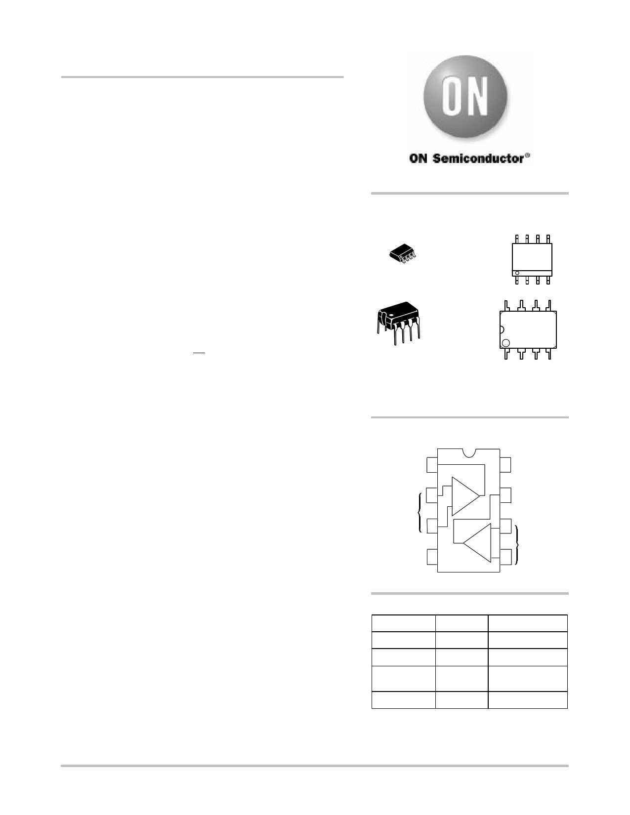
The MC33077 is available in plastic DIP and SOIC−8 packages (P
and D suffixes).
Features
• Low Voltage Noise: 4.4 nV/ǸHz @ 1.0 kHz
• Low Input Offset Voltage: 0.2 mV
• Low TC of Input Offset Voltage: 2.0 mV/°C
•
High Gain Bandwidth Product: 37 MHz @ 100 kHz
www.DataSheet4U.com
• High AC Voltage Gain: 370 @ 100 kHz
1850 @ 20 kHz
• Unity Gain Stable: with Capacitance Loads to 500 pF
• High Slew Rate: 11 V/ms
• Low Total Harmonic Distortion: 0.007%
• Large Output Voltage Swing: +14 V to −14.7 V
• High DC Open Loop Voltage Gain: 400 k (112 dB)
• High Common Mode Rejection: 107 dB
• Low Power Supply Drain Current: 3.5 mA
• Dual Supply Operation: ±2.5 V to ±18 V
• Pb−Free Package is Available
© Semiconductor Components Industries, LLC, 2004
March, 2004 − Rev. 5
1
http://onsemi.com
8
1
8
1
SOIC−8
D SUFFIX
CASE 751
MARKING
DIAGRAMS
8
33077
ALYW
1
8
PDIP−8
P SUFFIX
CASE 626
MC33077P
AWL
YYWW
1
A = Assembly Location
WL, L = Wafer Lot
YY, Y = Year
WW, W = Work Week
PIN CONNECTIONS
Output 1 1
Inputs 1
2
3
VEE 4
8 VCC
−
1 7 Output 2
+
6
−
2
+5
Inputs 2
(Dual, Top View)
ORDERING INFORMATION
Device
Package
Shipping†
MC33077D
SOIC−8
98 Units/Rail
MC33077DR2
MC33077DR2G
SOIC−8
SOIC−8
(Pb−Free)
2500 Tape & Reel
2500 Tape & Reel
MC33077P
PDIP−8
50 Units/Rail
†For information on tape and reel specifications,
including part orientation and tape sizes, please
refer to our Tape and Reel Packaging Specifications
Brochure, BRD8011/D.
Publication Order Number:
MC33077/D
1 page 
MC33077
1000
VCC = +15 V
800
VEE = −15 V
VCM = 0 V
600
400
200
1.0
0.5
0
−0.5
0
−55 −25 0 25 50 75 100 125
TA, AMBIENT TEMPERATURE (°C)
Figure 4. Input Bias Current
versus Temperature
−1.0
−55
VCC = +15 V
VEE = −15 V
RS = 10 W
VCM = 0 V
AV = +1.0
−25 0 25 50 75
TA, AMBIENT TEMPERATURE (°C)
100
Figure 5. Input Offset Voltage
versus Temperature
125
600
500
400
300
200
100
0
−15
VCC = +15 V
VEE = −15 V
TA = 25°C
−10 −5.0 0 5.0 10
VCM, COMMON MODE VOLTAGE (V)
Figure 6. Input Bias Current versus
Common Mode Voltage
15
VCC 0.0
VCC −0.5
+VCM
VCC −1.0
VCC −1.5
VEE +1.5
VEE +1.0
Input
Voltage
Range
VCC = +3.0 V to +15 V
VEE = −3.0 V to −15 V
D VIO = 5.0 mV
VO = 0 V
VEE +0.5
VEE +0.0
−55
−VCM
−25 0 25 50 75
TA, AMBIENT TEMPERATURE (°C)
100 125
Figure 7. Input Common Mode Voltage Range
versus Temperature
VCC 0
VCC −2
−55°C
VCC −4
25°C
125°C
125°C
VEE +4 25°C
VEE +2 −55°C
VCC = +15 V
VEE = −15 V
VEE 0 0
0.5 1.0 1.5 2.0 2.5
RL, LOAD RESISTANCE TO GROUND (kW)
3.0
Figure 8. Output Saturation Voltage versus
Load Resistance to Ground
50
40
Sink
30
Source
20
VCC = +15 V
VEE = −15 V
VID = ±1.0 V
RL < 100 W
10
−55
−25 0 25 50 75
TA, AMBIENT TEMPERATURE (°C)
100
Figure 9. Output Short Circuit Current
versus Temperature
125
http://onsemi.com
5
5 Page 
MC33077
APPLICATIONS INFORMATION
The MC33077 is designed primarily for its low noise, low
offset voltage, high gain bandwidth product and large output
swing characteristics. Its outstanding high frequency
gain/phase performance make it a very attractive amplifier for
high quality preamps, instrumentation amps, active filters and
other applications requiring precision quality characteristics.
The MC33077 utilizes high frequency lateral PNP input
transistors in a low noise bipolar differential stage driving a
compensated Miller integration amplifier. Dual−doublet
frequency compensation techniques are used to enhance the
gain bandwidth product. The output stage uses an all NPN
transistor design which provides greater output voltage
swing and improved frequency performance over more
conventional stages by using both PNP and NPN transistors
(Class AB). This combination produces an amplifier with
superior characteristics.
Through precision component matching and innovative
current mirror design, a lower than normal temperature
coefficient of input offset voltage (2.0 mV/°C as opposed to
10 mV/°C), as well as low input offset voltage, is accomplished.
The minimum common mode input range is from 1.5 V
below the positive rail (VCC) to 1.5 V above the negative rail
(VEE). The inputs will typically common mode to within
1.0 V of both negative and positive rails though degradation
in offset voltage and gain will be experienced as the common
mode voltage nears either supply rail. In practice, though not
recommended, the input voltage may exceed VCC by
approximately 3.0 V and decrease below the VEE by
approximately 0.6 V without causing permanent damage to
the device. If the input voltage on either or both inputs is less
than approximately 0.6 V, excessive current may flow, if not
limited, causing permanent damage to the device.
The amplifier will not latch with input source currents up
to 20 mA, though in practice, source currents should be
limited to 5.0 mA to avoid any parametric damage to the
device. If both inputs exceed VCC, the output will be in the
high state and phase reversal may occur. No phase reversal
will occur if the voltage on one input is within the common
mode range and the voltage on the other input exceeds VCC.
Phase reversal may occur if the input voltage on either or
both inputs is less than 1.0 V above the negative rail. Phase
reversal will be experienced if the voltage on either or both
inputs is less than VEE.
Through the use of dual−doublet frequency compensation
techniques, the gain bandwidth product has been greatly
enhanced over other amplifiers using the conventional
single pole compensation. The phase and gain error of the
amplifier remains low to higher frequencies for fixed
amplifier gain configurations.
With the all NPN output stage, there is minimal swing loss
to the supply rails, producing superior output swing, no
crossover distortion and improved output phase symmetry
with output voltage excursions (output phase symmetry
being the amplifiers ability to maintain a constant phase
relation independent of its output voltage swing). Output
phase symmetry degradation in the more conventional PNP
and NPN transistor output stage was primarily due to the
inherent cut−off frequency mismatch of the PNP and NPN
transistors used (typically 10 MHz and 300 MHz,
respectively), causing considerable phase change to occur as
the output voltage changes. By eliminating the PNP in the
output, such phase change has been avoided and a very
significant improvement in output phase symmetry as well
as output swing has been accomplished.
The output swing improvement is most noticeable when
operation is with lower supply voltages (typically 30% with
± 5.0 V supplies). With a 10 k load, the output of the
amplifier can typically swing to within 1.0 V of the positive
rail (VCC), and to within 0.3 V of the negative rail (VEE),
producing a 28.7 Vpp signal from ±15 V supplies. Output
voltage swing can be further improved by using an output
pull−up resistor referenced to the VCC. Where output signals
are referenced to the positive supply rail, the pull−up resistor
will pull the output to VCC during the positive swing, and
during the negative swing, the NPN output transistor
collector will pull the output very near VEE. This
configuration will produce the maximum attainable output
signal from given supply voltages. The value of load
resistance used should be much less than any feedback
resistance to avoid excess loading and allow easy pull−up of
the output.
Output impedance of the amplifier is typically less than
50 W at frequencies less than the unity gain crossover
frequency (see Figure 19). The amplifier is unity gain stable
with output capacitance loads up to 500 pF at full output
swing over the −55° to +125°C temperature range. Output
phase symmetry is excellent with typically 4°C total phase
change over a 20 V output excursion at 25°C with a 2.0 kW
and 100 pF load. With a 2.0 kW resistive load and no
capacitance loading, the total phase change is approximately
one degree for the same 20 V output excursion. With a
2.0 kW and 500 pF load at 125°C, the total phase change is
typically only 10°C for a 20 V output excursion (see
Figure 28).
As with all amplifiers, care should be exercised to insure
that one does not create a pole at the input of the amplifier
which is near the closed loop corner frequency. This becomes
a greater concern when using high frequency amplifiers since
it is very easy to create such a pole with relatively small values
of resistance on the inputs. If this does occur, the amplifier’s
phase will degrade severely causing the amplifier to become
unstable. Effective source resistances, acting in conjunction
with the input capacitance of the amplifier, should be kept to
a minimum to avoid creating such a pole at the input (see
Figure 32). There is minimal effect on stability where the
created input pole is much greater than the closed loop corner
frequency. Where amplifier stability is affected as a result of
a negative feedback resistor in conjunction with the
http://onsemi.com
11
11 Page | ||
| Páginas | Total 14 Páginas | |
| PDF Descargar | [ Datasheet MC33077.PDF ] | |
Hoja de datos destacado
| Número de pieza | Descripción | Fabricantes |
| MC33071 | (MC33071 / MC33072 / MC33074) HIGH BANDWIDTH SINGLE SUPPLY OPERATIONAL AMPLIFIERS | Motorola Semiconductors |
| MC33071 | Operational Amplifiers | ON Semiconductor |
| MC33071A | Operational Amplifiers | ON Semiconductor |
| MC33072 | (MC33071 / MC33072 / MC33074) HIGH BANDWIDTH SINGLE SUPPLY OPERATIONAL AMPLIFIERS | Motorola Semiconductors |
| Número de pieza | Descripción | Fabricantes |
| SLA6805M | High Voltage 3 phase Motor Driver IC. |
Sanken |
| SDC1742 | 12- and 14-Bit Hybrid Synchro / Resolver-to-Digital Converters. |
Analog Devices |
|
DataSheet.es es una pagina web que funciona como un repositorio de manuales o hoja de datos de muchos de los productos más populares, |
| DataSheet.es | 2020 | Privacy Policy | Contacto | Buscar |