|
|
|
PDF IRS2168DPBF Data sheet ( Hoja de datos )
| Número de pieza | IRS2168DPBF | |
| Descripción | ADVANCED PFC + BALLAST CONTROL IC | |
| Fabricantes | International Rectifier | |
| Logotipo | ||
Hay una vista previa y un enlace de descarga de IRS2168DPBF (archivo pdf) en la parte inferior de esta página. Total 21 Páginas | ||
|
No Preview Available !
www.DataSheet4U.com
Data Sheet No. PD60310
IRS2168D(S)PbF
ADVANCED PFC + BALLAST CONTROL IC
Features
PFC, ballast control and 600 V half-bridge driver in one IC
Critical-conduction mode boost-type PFC
Programmable PFC over-current protection
Programmable half-bridge over-current protection
Programmable preheat frequency
Programmable preheat time
Programmable ignition ramp
Programmable run frequency
Closed-loop ignition current regulation
RoHs compliant
Description
The IRS2168D is a fully integrated, fully protected 600 V
ballast control IC designed to drive all types of fluorescent
lamps. The IRS2168D is based on the popular IR2166
control IC with additional improvements to increase ballast
performance. The PFC circuitry operates in critical
conduction mode and provides high PF, low THD and DC
bus regulation. The IRS2168D features include
programmable preheat and run frequencies, programmable
preheat time, programmable PFC over-current protection,
closed-loop half-bridge ignition current regulation, and
programmable end-of-life protection. Comprehensive
protection features such as protection from failure of a lamp
to strike, filament failures, end-of-life protection, DC bus
undervoltage reset as well as an automatic restart function,
have been included in the design.
Fixed internal 1.6 µs HO and LO deadtime
Voltage-controlled oscillator (VCO)
End-of-life window comparator pin
Internal 65-event current sense up/down fault counter
DC bus undervoltage reset
Lamp removal/auto-restart shutdown pin
Internal bootstrap MOSFET
Internal 15.6 V Zener clamp diode on Vcc
Micropower startup (250 µA)
Latch immunity and ESD protection
System Features
One-chip ballast control solution
Wide range PFC for universal input and multi-lamp ballasts
Ultra low THD
Closed-loop ignition regulation for reliable lamp ignition
End-of-Life window comparator with internal OTA
Lamp removal/auto-restart function
Fault counter for robust noise immunity
Brown-out protection and reset
Internal bootstrap MOSFET
Packages
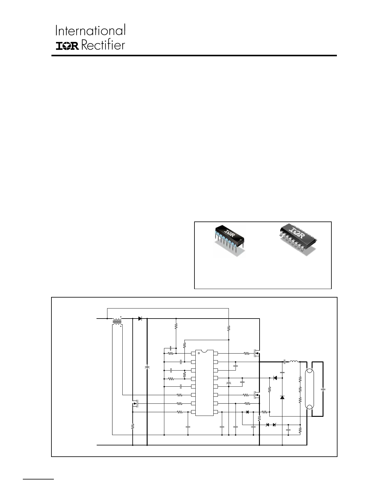
Application Diagram (Typical Only)
16-Lead PDIP
IRS2168DPbF
16-Lead SOIC
IRS2168DSPbF
+ Rectified AC Line
D BUS
R VBUS1
R SUPPLY
- Rectified AC Line
C BUS +
M3
R OC
C VBUS
RCPH
R VBUS C PH
VBUS
1
CPH
2
C VCO
R
R
FMIN
RPH
VCO
3
FMIN
4
CCOMP
COMP
5
R1
R GPFC
ZX
76
PFC
7
R2 OC
8
C OC
HO
16
R GHS
VS
15
VB
14
C BOOT
VCC
13
COM
12
LO
11
CS
10
SD/EOL
9
CVCC1
CVCC2
R GLS
R3
D1
C SD1
CCS C SD2
M1
CBLOCK LRES
D CP1
C SNUB
R6
R4
M2
D CP2
R5
RCS
D2 D3
R7
R8
C EOL R 9
CRES
* Please note that this datasheet contains advanced information that could change before the product is released to production.
www.irf.com
Page 1
1 page 
IRS2168D(S)PbF
Electrical Characteristics (cont’d)
VCC = VBS = VBIAS=14 V +/- 0.25 V, CLO = CHO = CPFC = 1000 pF, RFMIN = 42.2 kΩ, RPH = N/C, VCPH = VVCO = 0 V,
VSD/EOL = VCOMP = VCS = VOC = VBUS = VZX = 0 V, TA=25 oC unless otherwise specified.
Symbol
Definition
Min Typ Max Units Test Conditions
Ballast Control Oscillator Characteristics
fOSC, RUN Half-bridge oscillator run frequency
fOSC, PH
D
td, LO
td, HO
VFMIN
Half-bridge oscillator preheat frequency
Oscillator duty cycle
LO output deadtime
HO output deadtime
FMIN pin voltage
42.5
81
---
1.1
1.1
1.9
44.5
85
50
1.6
1.6
2.0
46.5
89
---
2.1
2.1
2.1
kHz
%
µs
V
MODE = RUN
RPH = 42.2 kΩ,
MODE = PREHEAT
VCC = 14.0 V
Ballast Control Preheat, Ignition and Run Mode Characteristics
VCPHEOP+
CPH pin end of preheat rising threshold
voltage
8.8 9.3 9.8
VCPHSOI-
CPH pin start of ignition falling threshold
voltage
4.6 4.9
5.2
VVCOPH VCO pin preheat mode voltage
--- 0
---
VVCOIGN VCO pin ignition mode voltage
---
(Open
Drain)
---
IVCOIGN
VCO pin ignition regulation discharge
current
--- 0.6 ---
VCPHRUN+ CPH pin run mode rising threshold voltage 8.8
9.3
VVCORUN VCO pin run mode voltage
---
(Open
Drain)
Ballast Control Protection Circuitry Characteristics
VCSTH+ CS pin over-current sense threshold
1.1 1.2
nEVENTS
VSDTH+
VSDTH-
CS pin fault counter number of events
SD pin rising non-latched shutdown
threshold voltage
SD pin falling reset threshold voltage
30 65
4.7 5.2
2.5 3.0
VEOLBIAS
VEOLTH+
VEOLTH-
EOL pin internal bias voltage
EOL pin rising latched shutdown threshold
voltage
EOL pin falling latched shutdown threshold
voltage
1.9
2.85
0.9
2.0
3.0
1.0
IEOL, SOURCE EOL pin OTA output sourcing current
--- 10
IEOL, SINK EOL pin OTA output sinking current
VCPHFLT CPH pin fault mode voltage
VVCOFLT VCO pin fault mode voltage
VFMINFLT FMIN pin fault mode voltage
--- -10
--- 0
9.8
---
1.3
100
5.7
3.5
2.1
3.15
1.1
---
---
---
V
MODE = PREHEAT
MODE = IGNITION, VCS
< VCSTH+
MODE = IGNITION,
mA VVCO = 1 V,
VCS > VCSTH+
MODE = IGNITION
V
MODE = RUN
V
---
MODE = PREHEAT or
RUN
V
MODE = RUN
MODE = RUN
MODE = PREHEAT
µA VEOL = 1.5 V
MODE = PREHEAT
VEOL = 2.5 V
V MODE = FAULT
www.irf.com
Page 5
5 Page 
IRS2168D(S)PbF
I. Ballast Section
Functional Description
Undervoltage Lockout Mode (UVLO)
The undervoltage lockout mode (UVLO) is defined as the
state the IC is in when VCC is below the turn-on threshold
of the IC. To identify the different modes of the IC, refer to
the State Diagram shown on page 3 of this document. The
IRS2168D undervoltage lockout is designed to maintain
an ultra low supply current of 250 µA (IQCCUV), and to
guarantee the IC is fully functional before the high- and
low-side output drivers are activated. Figure 1 shows an
efficient supply voltage using the micro-power start-up
current of the IRS2168D together with a snubber charge
pump from the half-bridge output (RVCC, CVCC1, CVCC2,
CSNUB, DCP1 and DCP2).
VRECT (+)
VBUS (+)
VBUS(-)
HO
16
VS
15
RVCC
RHO
MHS
IC COM
BSFET
CONTROL
BSFET
VB
14
VCC
13
CBS
R2
C VCC2 R1 DCP2
COM C VCC1
12
LO
11
CS
10
RLO
R3
MLS
IRS2168D
CCS
RCS
To Load
C SNUB
DCP1
Load
Return
Figure 1: Start-up and supply circuitry
The VCC capacitors (CVCC1 and CVCC2) are charged by the
current through supply resistor (RVCC) minus the start-up
current drawn by the IC. This resistor is chosen to set the
desired AC line input voltage turn-on threshold for the
ballast. When the voltage at VCC exceeds the IC start-up
threshold (VCCUV+) and the SD pin is below 3.0 V (VSDTH-),
the IC turns on and LO begins to oscillate. The capacitors
at VCC begin to discharge due to the increase in IC
operating current (Fig. 2). The high-side supply voltage,
VB-VS, begins to increase as capacitor CBS is charged
through the internal bootstrap MOSFET during the LO on-
time of each LO switching cycle. When the VB-VS voltage
exceeds the high-side start-up threshold (VBSUV+), HO then
begins to oscillate. This may take several cycles of LO to
charge VB-VS above VBSUV+ due to RDSon of the internal
bootstrap MOSFET.
VC1
CVCC
DISCHARGE
VUVLO+
VHYST
VUVLO-
INTERNAL VCC
ZENER CLAMP VOLTAGE
DISCHARGE
TIME
RVCC & CVCC1,2
TIME
CONSTANT
CHARGE PUMP
OUTPUT
t
Figure 2: VCC supply voltage
When LO and HO are both oscillating, the external
MOSFETs (MHS and MLS) are turned on and off with a
50% duty cycle and a non-overlapping deadtime of 1.6
µs (td). The half-bridge output (pin VS) begins to switch
between the DC bus voltage and COM. During the
deadtime between the turn-off of LO and the turn-on of
HO, the half-bridge output voltage transitions from COM
to the DC bus voltage at a dV/dt rate determined by the
snubber capacitor (CSNUB). As the snubber capacitor
charges, current will flow through the charge pump diode
(DCP2) to VCC. After several switching cycles of the half-
bridge output, the charge pump and the internal 15.6 V
Zener clamp of the IC take over as the supply voltage.
Capacitor CVCC2 supplies the IC current during the VCC
discharge time and should be large enough such that
VCC does not decrease below UVLO- before the charge
pump takes over. Capacitor CVCC1 is required for noise
filtering and must be placed as close as possible and
directly between VCC and COM, and should not be lower
than 0.1 µF Resistors R1 and R2 are recommended for
limiting high currents that can flow to VCC from the charge
pump during hard-switching of the half-bridge or during
lamp ignition. The internal bootstrap MOSFET and
supply capacitor (CBS) comprise the supply voltage for
the high side driver circuitry. During UVLO mode, the
high- and low-side driver outputs HO and LO are both
low, the internal oscillator is disabled, and pin CPH is
connected internally to COM for resetting the preheat
time.
www.irf.com
Page 11
11 Page | ||
| Páginas | Total 21 Páginas | |
| PDF Descargar | [ Datasheet IRS2168DPBF.PDF ] | |
Hoja de datos destacado
| Número de pieza | Descripción | Fabricantes |
| IRS2168DPBF | ADVANCED PFC + BALLAST CONTROL IC | International Rectifier |
| Número de pieza | Descripción | Fabricantes |
| SLA6805M | High Voltage 3 phase Motor Driver IC. |
Sanken |
| SDC1742 | 12- and 14-Bit Hybrid Synchro / Resolver-to-Digital Converters. |
Analog Devices |
|
DataSheet.es es una pagina web que funciona como un repositorio de manuales o hoja de datos de muchos de los productos más populares, |
| DataSheet.es | 2020 | Privacy Policy | Contacto | Buscar |