|
|
|
PDF AD6624 Data sheet ( Hoja de datos )
| Número de pieza | AD6624 | |
| Descripción | 80 MSPS Digital Receive Signal Processor | |
| Fabricantes | Analog Devices | |
| Logotipo | ||
Hay una vista previa y un enlace de descarga de AD6624 (archivo pdf) en la parte inferior de esta página. Total 30 Páginas | ||
|
No Preview Available !
www.DataSheet4U.com
a
Four-Channel, 80 MSPS Digital
Receive Signal Processor (RSP)
FEATURES
80 MSPS Wide Band Inputs (14 Linear Bits Plus 3 RSSI)
Dual High Speed Data Input Ports
Four Independent Digital Receivers in Single Package
Digital Resampling for Noninteger Decimation Rates
Programmable Decimating FIR Filters
Programmable Attenuator Control for Clip Prevention
and External Gain Ranging via Level Indicator
Flexible Control for Multicarrier and Phased Array
3.3 V I/O, 2.5 V CMOS Core
User-Configurable Built-In Self-Test (BIST) Capability
JTAG Boundary Scan
APPLICATIONS
Multicarrier, Multimode Digital Receivers GSM, IS136,
EDGE, PHS, IS95
Micro and Pico Cell Systems
Wireless Local Loop
Smart Antenna Systems
Software Radios
In-Building Wireless Telephony
PRODUCT DESCRIPTION
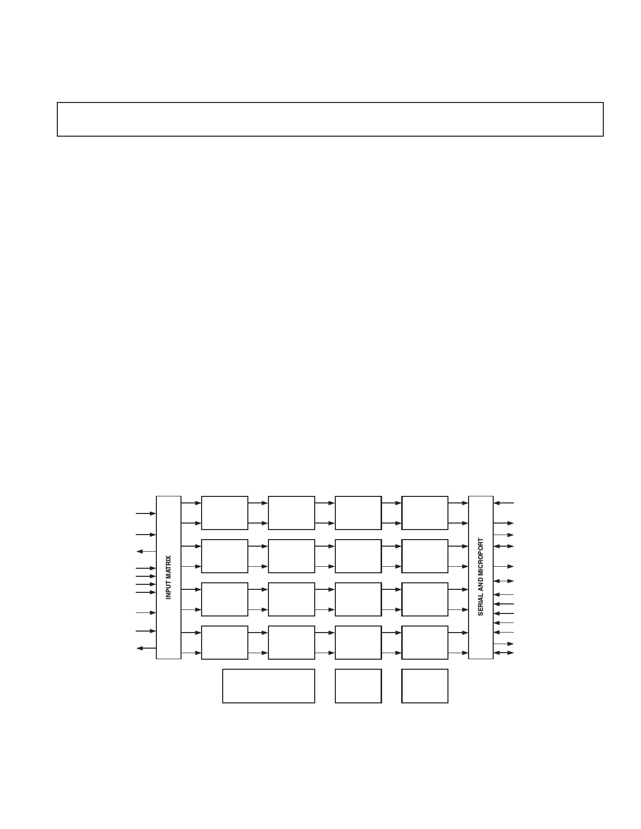
The AD6624 is a four-channel (quad) digital receive signal
processor (RSP) with four cascaded signal-processing elements:
a frequency translator, two fixed-coefficient decimating filters,
and a programmable-coefficient decimating filter.
AD6624
The AD6624 is part of Analog Devices’ SoftCell® multicarrier
transceiver chipset designed for compatibility with Analog
Devices’ family of high sample rate IF sampling ADCs (AD6640/
AD6644 12- and 14-bit). The SoftCell receiver comprises a
digital receiver capable of digitizing an entire spectrum of
carriers and digitally selecting the carrier of interest for tuning
and channel selection. This architecture eliminates redundant
radios in wireless base station applications.
High dynamic range decimation filters offer a wide range of
decimation rates. The RAM-based architecture allows easy
reconfiguration for multimode applications.
The decimating filters remove unwanted signals and noise from
the channel of interest. When the channel of interest occupies less
bandwidth than the input signal, this rejection of out-of-band
noise is called “processing gain.” By using large decimation
factors, this “processing gain” can improve the SNR of the
ADC by 30 dB or more. In addition, the programmable RAM
coefficient filter allows antialiasing, matched filtering, and
static equalization functions to be combined in a single, cost-
effective filter.
The AD6624 is compatible with standard ADC converters such
as the AD664x, AD9042, AD943x, and the AD922x families of
data converters. The AD6624 is also compatible with the AD6600
Diversity ADC, providing a cost and size reduction path.
INA[13:0]
EXPA[2:0]
IENA
LIA-A
LIA-B
SYNCA
SYNCB
SYNCC
SYNCD
INB[13:0]
EXPB[2:0]
IENB
LIB-A
LIB-B
CH A
FUNCTIONAL BLOCK DIAGRAM
NCO
16 BITS
18 BITS
rCIC2
RESAMPLER
CIC5
20 BITS
24 BITS
RAM
COEFFICIENT
FILTER
CH B
NCO
rCIC2
RESAMPLER
CIC5
RAM
COEFFICIENT
FILTER
CH C
NCO
rCIC2
RESAMPLER
CIC5
RAM
COEFFICIENT
FILTER
CH D
NCO
rCIC2
RESAMPLER
CIC5
RAM
COEFFICIENT
FILTER
SDIN[3:0]
SDO[3:0]
DR[3:0]
SDFS[3:0]
SDFE[3:0]
SCLK[3:0]
MODE
DS(RD)
CS
RW (WR)
DTACK(RDY)
A[2:0]
D[7:0]
EXTERNAL SYNC
CIRCUITRY
JTAG
INTERFACE
BUILT-IN
SELF-TEST
REV. B
Information furnished by Analog Devices is believed to be accurate and
reliable. However, no responsibility is assumed by Analog Devices for its
use, nor for any infringements of patents or other rights of third parties that
may result from its use. No license is granted by implication or otherwise
under any patent or patent rights of Analog Devices. Trademarks and
registered trademarks are the property of their respective owners.
One Technology Way, P.O. Box 9106, Norwood, MA 02062-9106, U.S.A.
Tel: 781/329-4700
www.analog.com
Fax: 781/326-8703 © 2004 Analog Devices, Inc. All rights reserved.
1 page 
MICROPROCESSOR PORT TIMING CHARACTERISTICS1, 2
Parameter (Conditions)
Temp
Test
Level
MICROPROCESSOR PORT, MODE INM (MODE = 0)
MODE INM Write Timing:
tSC
tHC
tHWR
tSAM
tHAM
tDRDY
tACC
Control3 to ↑CLK Setup Time
Control3 to ↑CLK Hold Time
WR(RW) to RDY(DTACK) Hold Time
Address/Data to WR(RW) Setup Time
Address/Data to RDY(DTACK) Hold Time
WR(RW) to RDY(DTACK) Delay
WR(RW) to RDY(DTACK) High Delay
MODE INM Read Timing:
tSC Control3 to ↑CLK Setup Time
tHC Control3 to ↑CLK Hold Time
tSAM Address to RD(DS) Setup Time
tHAM
tDRDY
tACC
Address to Data Hold Time
RD(DS) to RDY(DTACK) Delay
RD(DS) to RDY(DTACK) High Delay
MICROPROCESSOR PORT, MODE MNM (MODE = 1)
Full
Full
Full
Full
Full
Full
Full
Full
Full
Full
Full
Full
Full
IV
IV
IV
IV
IV
IV
IV
IV
IV
IV
IV
IV
IV
MODE MNM Write Timing:
tSC
tHC
tHDS
tHRW
tSAM
tHAM
tACC
Control3 to ↑CLK Setup Time
Control3 to ↑CLK Hold Time
DS(RD) to DTACK(RDY) Hold Time
RW(WR) to DTACK(RDY) Hold Time
Address/Data to RW(WR) Setup Time
Address/Data to RW(WR) Hold Time
RW(WR) to DTACK(RDY) Low Delay
Full IV
Full IV
Full IV
Full IV
Full IV
Full IV
Full IV
MODE MNM Read Timing:
tSC Control3 to ↑CLK Setup Time
tHC Control3 to ↑CLK Hold Time
tSAM Address to DS(RD) Setup Time
tHAM
Address to Data Hold Time
tZD Data Three-State Delay
tACC DS(RD) to DTACK(RDY) Low Delay
Full IV
Full IV
Full IV
Full IV
Full IV
Full IV
NOTES
1All timing specifications valid over VDD range of 2.375 V to 2.675 V and VDDIO range of 3.0 V to 3.6 V.
2CLOAD = 40 pF on all outputs unless otherwise specified.
3Specification pertains to control signals: RW, (WR), DS, (RD), CS.
Specifications subject to change without notice.
AD6624
AD6624AS
Min Typ Max
Unit
5.5
1.0
8.0
–0.5
7.0
4.0
4 × tCLK
5 × tCLK
9 × tCLK
ns
ns
ns
ns
ns
ns
ns
4.0
2.0
0.0
7.0
4.0
8 × tCLK
10 × tCLK 13 × tCLK
ns
ns
ns
ns
ns
ns
5.5
1.0
8.0
8.0
–0.5
7.0
4 × tCLK
5 × tCLK
9 × tCLK
ns
ns
ns
ns
ns
ns
ns
4.0
2.0
8.0
0.0
7.0
8 × tCLK
10 × tCLK 13 × tCLK
ns
ns
ns
ns
ns
ns
REV. B
–5–
5 Page 
Pin No.
1, 12, 38, 50, 65, 76, 102, 113
2–6
7, 17, 32, 44, 54, 81, 96, 118
8
9
10
11
13
14–16
18–21
22, 59, 71, 86, 108, 123
23–26
27, 39, 64, 91, 103, 128
28–31
33–34
35
36
37
40
41
42
43
45
46–49
51–53
55
56
57
58
60
61–63
66
67
68
69
70
72
73–75
77
78
79–80
82–83
84
85
87
88
89
90
AD6624
PIN FUNCTION DESCRIPTIONS
Mnemonic
VSS
INB[5:1]1
VDD
INB01
IENB2
LIB-B
LIB-A
CLK
EXPA[0:2]1
INA[13:10]1
VDDIO
INA[9:6]1
VSSIO
INA[5:2]1
INA[1:0]1
IENA2
LIA-B
LIA-A
SYNCD1
SYNCC1
SYNCB1
SYNCA1
RESET
D[7:4]
D[3:1]
D0
DS(RD)
DTACK(RDY)2
RW(WR)
MODE
A[2:0]
CS1
TRST2
TCLK1
TMS2
TDO
TDI2
CHIP_ID[3:1]1
CHIP_ID01
SBM01
SDIV[3:2]1
SDIV[1:0]1
SCLK01
SDFS01
SDO01
SDIN01
SDFE0
DR0
Type
G
I
P
I
I
O
O
I
I
I
P
I
G
I
I
I
O
O
I
I
I
I
I
I/O/T
I/O/T
I/O/T
I
O/T
I
I
I
I
I
I
I
O/T
I
I
I
I
I
I
I/O
I/O
O/T
I
O
O
Function
Ground
B Input Data (Mantissa)
2.5 V Supply
B Input Data (Mantissa)—LSB
Input Enable—Input B
Level Indicator—Input B, Interleaved—Data B
Level Indicator—Input B, Interleaved—Data A
Input Clock
A Input Data (Exponent)
A Input Data (Mantissa)
3.3 V Supply
A Input Data (Mantissa)
Ground
A Input Data (Mantissa)
A Input Data (Mantissa)
Input Enable—Input A
Level Indicator—Input A, Interleaved—Data B
Level Indicator—Input A, Interleaved—Data A
All Sync Pins Go to All Four Output Channels
All Sync Pins Go to All Four Output Channels
All Sync Pins Go to All Four Output Channels
All Sync Pins Go to All Four Output Channels
Active Low Reset Pin
Bidirectional Microport Data
Bidirectional Microport Data
Bidirectional Microport Data—LSB
Active Low Data Strobe (Active Low Read)
Active Low Data Acknowledge (Microport Status Bit)
Read Write (Active Low Write)
Intel or Motorola Mode Select
Microport Address Bus
Chip Select
Test Reset Pin
Test Clock Input
Test Mode Select Input
Test Data Output
Test Data Input
Chip ID Selector
Chip ID Selector—LSB
Serial Bus Master—Channel 0 Only
Serial Clock Divisor—Channel 0
Serial Clock Divisor—Channel 0
Bidirectional Serial Clock—Channel 0
Bidirectional Serial Data Frame Sync—Channel 0
Serial Data Output—Channel 0
Serial Data Input—Channel 0
Serial Data Frame End—Channel 0
Output Data Ready Indicator—Channel 0
REV. B
–11–
11 Page | ||
| Páginas | Total 30 Páginas | |
| PDF Descargar | [ Datasheet AD6624.PDF ] | |
Hoja de datos destacado
| Número de pieza | Descripción | Fabricantes |
| AD6620 | 65 MSPS Digital Receive Signal Processor | Analog Devices |
| AD6622 | Four-Channel/ 75 MSPS Digital Transmit Signal Processor TSP | Analog Devices |
| AD6623 | 4-Channel/ 104 MSPS Digital Transmit Signal Processor TSP | Analog Devices |
| AD6624 | 80 MSPS Digital Receive Signal Processor | Analog Devices |
| Número de pieza | Descripción | Fabricantes |
| SLA6805M | High Voltage 3 phase Motor Driver IC. |
Sanken |
| SDC1742 | 12- and 14-Bit Hybrid Synchro / Resolver-to-Digital Converters. |
Analog Devices |
|
DataSheet.es es una pagina web que funciona como un repositorio de manuales o hoja de datos de muchos de los productos más populares, |
| DataSheet.es | 2020 | Privacy Policy | Contacto | Buscar |