|
|
|
PDF AD8202 Data sheet ( Hoja de datos )
| Número de pieza | AD8202 | |
| Descripción | Single-Supply Difference Amplifier | |
| Fabricantes | Analog Devices | |
| Logotipo | ||
Hay una vista previa y un enlace de descarga de AD8202 (archivo pdf) en la parte inferior de esta página. Total 21 Páginas | ||
|
No Preview Available !
Data Sheet
High Common-Mode Voltage,
Single-Supply Difference Amplifier
AD8202
FEATURES
High common-mode voltage range
−6 V to +28 V at a 5 V supply voltage
Operating temperature range: −40°C to +125°C
Supply voltage range: 3.5 V to 12 V
Low-pass filter (1-pole or 2-pole)
Excellent ac and dc performance
±1 mV voltage offset
±1 ppm/°C typical gain drift
80 dB CMRR min dc to 10 kHz
Qualified for automotive applications
APPLICATIONS
Transmission control
Diesel injection control
Engine management
Adaptive suspension control
Vehicle dynamics control
GENERAL DESCRIPTION
The AD8202 is a single-supply difference amplifier for amplifying
and low-pass filtering small differential voltages in the presence of a
large common-mode voltage (CMV). The input CMV range
extends from −6 V to +28 V at a typical supply voltage of 5 V.
The AD8202 is available in die and packaged form. The MSOP
and SOIC packages are specified over a wide temperature range,
from −40°C to +125°C, making the AD8202 well-suited for use
in many automotive platforms.
Automotive platforms demand precision components for
better system control. The AD8202 provides excellent ac and
dc performance keeping errors to a minimum in the user’s
system. Typical offset and gain drift in the SOIC package are
0.3 µV/°C and 1 ppm/°C, respectively. Typical offset and gain
drift in the MSOP package are 2 µV/°C and 1 ppm/°C, respec-
tively. The device also delivers a minimum CMRR of 80 dB
from dc to 10 kHz.
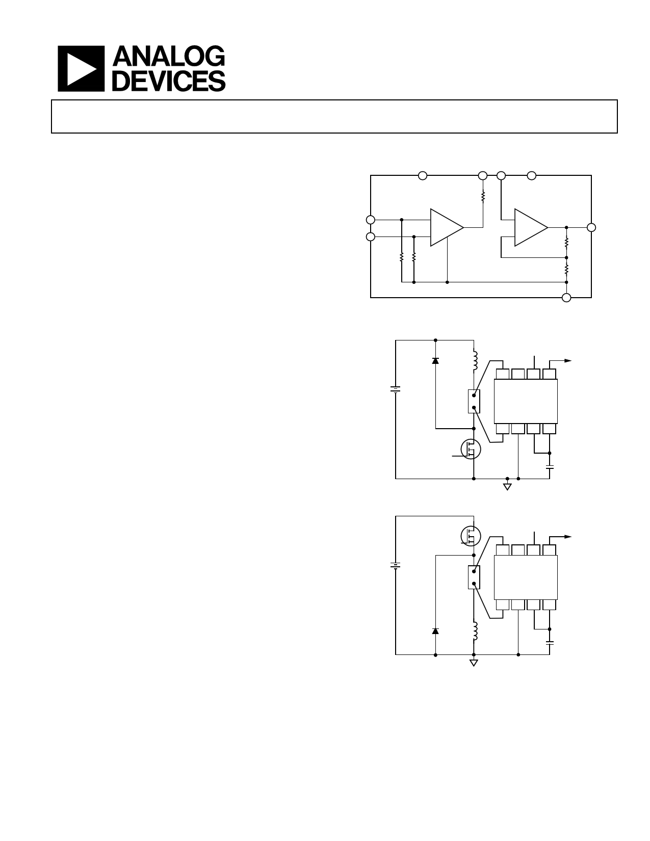
The AD8202 features an externally accessible 100 kΩ resistor
at the output of the Preamp A1 that can be used for low-pass
filter applications and for establishing gains other than 20.
FUNCTIONAL BLOCK DIAGRAMS
+IN 8
–IN 1
200kΩ
NC A1 A2
7 34
100kΩ
G = ×10
+IN
A1
–IN
200kΩ
+VS
6
AD8202
G = ×2
+IN
A2
–IN
10kΩ
5 OUT
10kΩ
NC = NO CONNECT
Figure 1. SOIC (R) Package Die Form
2
GND
BATTERY
CLAMP
DIODE
14V
4-TERM
SHUNT
INDUCTIVE
LOAD
5V
+IN NC +VS OUT
AD8202
OUTPUT
POWER
DEVICE
–IN GND A1 A2
BATTERY
COMMON
NC = NO CONNECT
Figure 2. High Line Current Sensor
POWER
DEVICE
5V
OUTPUT
+IN NC +VS OUT
14V
4-TERM
SHUNT
AD8202
–IN GND A1 A2
CLAMP
DIODE
INDUCTIVE
LOAD
COMMON
NC = NO CONNECT
Figure 3. Low Line Current Sensor
Rev. H
Document Feedback
Information furnished by Analog Devices is believed to be accurate and reliable. However, no
responsibilityisassumedbyAnalogDevices for itsuse,nor foranyinfringementsofpatentsor other
rights of third parties that may result from its use. Specifications subject to change without notice. No
license is granted by implication or otherwise under any patent or patent rights of Analog Devices.
Trademarksandregisteredtrademarksarethepropertyoftheirrespectiveowners.
One Technology Way, P.O. Box 9106, Norwood, MA 02062-9106, U.S.A.
Tel: 781.329.4700 ©2004–2013 Analog Devices, Inc. All rights reserved.
Technical Support
www.analog.com
1 page 
AD8202
ABSOLUTE MAXIMUM RATINGS
Table 2.
Parameter
Rating
Supply Voltage
12.5 V
Transient Input Voltage (400 ms)
44 V
Continuous Input Voltage (Common Mode) 35 V
Reversed Supply Voltage Protection
0.3 V
Operating Temperature Range
Die −40°C to +150°C
SOIC
−40°C to +125°C
MSOP
−40°C to +125°C
Storage Temperature
−65°C to +150°C
Output Short-Circuit Duration
Indefinite
Lead Temperature Range (Soldering, 10 sec) 300°C
Data Sheet
Stresses above those listed under Absolute Maximum Ratings
may cause permanent damage to the device. This is a stress
rating only; functional operation of the device at these or any
other conditions above those indicated in the operational
section of this specification is not implied. Exposure to absolute
maximum rating conditions for extended periods may affect
device reliability.
ESD CAUTION
Rev. H | Page 4 of 20
5 Page 
AD8202
35
TEMPERATURE = –40°C
30
25
20
15
10
5
0
VOS (µV)
Figure 30. VOS Distribution, SOIC, Temperature = −40°C
25
VSUPPLY = 5V
TEMPERATURE RANGE =
–40°C TO +25°C
20
15
10
5
0
VOS DRIFT (µV/°C)
Figure 31. Offset Drift Distribution, SOIC,
Temperature Range = −40°C to +25°C
25
VSUPPLY = 5V
TEMPERATURE RANGE =
25°C TO 85°C
20
15
10
5
0
VOS DRIFT (µV/°C)
Figure 32. Offset Drift Distribution, SOIC,
Temperature Range = 25°C to 85°C
Data Sheet
30
VSUPPLY = 5V
TEMPERATURE RANGE =
25 25°C TO 125°C
20
15
10
5
0
VOS DRIFT (µV/°C)
Figure 33. Offset Drift Distribution, SOIC,
Temperature Range = 25°C to 125°C
40
TEMPERATURE = 25°C
35
30
25
20
15
10
5
0
ERROR (%)
Figure 34. Gain Accuracy, SOIC, Temperature = 25°C
45
TEMPERATURE = 125°C
40
35
30
25
20
15
10
5
0
ERROR (%)
Figure 35. Gain Accuracy, SOIC, Temperature = 125°C
Rev. H | Page 10 of 20
11 Page | ||
| Páginas | Total 21 Páginas | |
| PDF Descargar | [ Datasheet AD8202.PDF ] | |
Hoja de datos destacado
| Número de pieza | Descripción | Fabricantes |
| AD820 | FET Input Op Amp | Analog Devices |
| AD8200 | High Common-Mode Voltage/ Single Supply Difference Amplifier | Analog Devices |
| AD8202 | Single-Supply Difference Amplifier | Analog Devices |
| AD8203 | Single-Supply Difference Amplifier | Analog Devices |
| Número de pieza | Descripción | Fabricantes |
| SLA6805M | High Voltage 3 phase Motor Driver IC. |
Sanken |
| SDC1742 | 12- and 14-Bit Hybrid Synchro / Resolver-to-Digital Converters. |
Analog Devices |
|
DataSheet.es es una pagina web que funciona como un repositorio de manuales o hoja de datos de muchos de los productos más populares, |
| DataSheet.es | 2020 | Privacy Policy | Contacto | Buscar |