|
|
|
PDF MT28F008B3 Data sheet ( Hoja de datos )
| Número de pieza | MT28F008B3 | |
| Descripción | (MT28F008B3 / MT28F800B3) FLASH MEMORY | |
| Fabricantes | Micron Technology | |
| Logotipo | ||
Hay una vista previa y un enlace de descarga de MT28F008B3 (archivo pdf) en la parte inferior de esta página. Total 30 Páginas | ||
|
No Preview Available !
www.DataSheet4U.com
FLASH MEMORY
8Mb
SMART 3 BOOT BLOCK FLASH MEMORY
MT28F008B3
MT28F800B3
3V Only, Dual Supply (Smart 3)
FEATURES
• Eleven erase blocks:
16KB/8K-word boot block (protected)
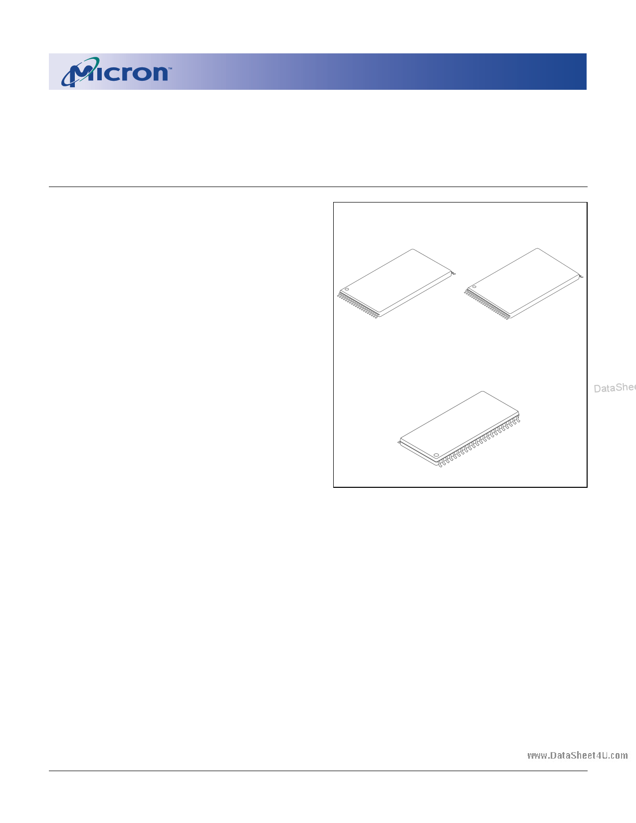
40-Pin TSOP Type I 48-Pin TSOP Type I
Two 8KB/4K-word parameter blocks
Eight main memory blocks
• Smart 3 technology (B3):
3.3V ±0.3V VCC
3.3V ±0.3V VPP application programming
5V ±10% VPP application/production programming1
• Compatible with 0.3µm Smart 3 device
• Advanced 0.18µm CMOS floating-gate process
• Address access time: 90ns
• 100,000 ERASE cycles
• Industry-standard pinouts
• Inputs and outputs are fully TTL-compatible
44-Pin SOP
• Automated write and erase algorithm
• Two-cycle WRITE/ERASE sequence
• TSOP, SOP and FBGA packaging options
DataSheet4U.com
• Byte- or word-wide READ and WRITE
(MT28F800B3):
1 Meg x 8/512K x 16
DataShee
OPTIONS
• Timing
90ns access
• Configurations
1 Meg x 8
512K x 16/1 Meg x 8
• Boot Block Starting Word Address
Top (7FFFFh)
Bottom (00000h)
• Operating Temperature Range
Commercial (0ºC to +70ºC)
Extended (-40ºC to +85ºC)
• Packages
40-pin TSOP Type I (MT28F008B3)
48-pin TSOP Type I (MT28F800B3)
44-pin SOP (MT28F800B3)
MARKING
-9
MT28F008B3
MT28F800B3
T
B
None
ET
VG
WG
SG
NOTE:
1. This generation of devices does not support 12V VPP
production programming; however, 5V VPP application
production programming can be used with no loss of
performance.
Part Number Example:
MT28F800B3WG-9 BET
DataSheet4U.com
GENERAL DESCRIPTION
The MT28F008B3 (x8) and MT28F800B3 (x16/x8) are
low-voltage, nonvolatile, electrically block-erasable (flash),
programmable memory devices containing 8,388,608 bits
organized as 524,288 words (16 bits) or 1,048,576 bytes (8
bits). Writing and erasing the device is done with a VPP
voltage of either 3.3V or 5V, while all operations are
performed with a 3.3V VCC. Due to process technology
advances, 5V VPP is optimal for application and production
programming. These devices are fabricated with Micron’s
advanced 0.18µm CMOS floating-gate process.
The MT28F008B3 and MT28F800B3 are organized
into eleven separately erasable blocks. To ensure that
critical firmware is protected from accidental erasure or
overwrite, the devices feature a hardware-protected
boot block. This block may be used to store code imple-
mented in low-level system recovery. The remaining
blocks vary in density and are written and erased with
no additional security measures.
Refer to Micron’s Web site (www.micron.com/flash)
for the latest data sheet.
8Mb Smart 3 Boot Block Flash Memory
Q10_3.p65 – Rev. 3, Pub. 10/01
1
©2001, Micron Technology, Inc.
PRODUCTS AND SPECIFICATIONS DISCUSSED HEREIN ARE SUBJECT TO CHANGE BY MICRON WITHOUT NOTICE.
DataSheet4 U .com
1 page 
www.DataSheet4U.com
8Mb
SMART 3 BOOT BLOCK FLASH MEMORY
TRUTH TABLE (MT28F800B3)1
et4U.com
FUNCTION
RP# CE# OE# WE# WP# BYTE# A0 A9 VPP DQ0–DQ7 DQ8–DQ14 DQ15/A - 1
Standby
H H X X X X X X X High-Z High-Z High-Z
RESET
L X X X X X X X X High-Z High-Z High-Z
READ
READ (word mode)
H L L H X H X X X Data-Out Data-Out Data-Out
READ (byte mode)
H L L H X L X X X Data-Out High-Z A-1
Output Disable
HL
WRITE/ERASE (EXCEPT BOOT BLOCK)2
H H X X X X X High-Z High-Z High-Z
ERASE SETUP
ERASE CONFIRM3
H L H L X X X X X 20h
H L H L X X X X VPPH D0h
X
X
X
X
WRITE SETUP
H L H L X X X X X 10h/40h X
X
WRITE (word mode)4
H L H L X H X X VPPH Data-In Data-In Data-In
WRITE (byte mode)4
H L H L X L X X VPPH Data-In
X
A-1
READ ARRAY5
H L H L X X XX X
FFh
X
X
WRITE/ERASE (BOOT BLOCK)2, 7
ERASE SETUP
H L H L X X X X X 20h
X
X
ERASE CONFIRM3
ERASE CONFIRM3, 6
WRITE SETUP
VHH L H L X X X X VPPH D0h
H L H L H X X X VPPH D0h
H L DaHtaSheLet4UX.comX X X X 10h/40h
X
X
X
X DataShee
X
X
WRITE (word mode)4
VHH L H L X H X X VPPH Data-In Data-In Data-In
WRITE (word mode)4, 6
H L H L H H X X VPPH Data-In Data-In Data-In
WRITE (byte mode)4
VHH L H L X L X X VPPH Data-In
X
A-1
WRITE (byte mode)4, 6
H L H L H L X X VPPH Data-In
X
A-1
READ ARRAY5
H L H L X X XX X
FFh
X
X
DEVICE IDENTIFICATION8, 9
Manufacturer Compatibility
(word mode)10
H L L H X H L VID X
89h
00h
–
Manufacturer Compatibility
(byte mode)
Device (word mode, top boot)10
HL
HL
L H X L L VID X
L H X H H VID X
89h High-Z
9Ch 88h
X
–
Device (byte mode, top boot)
Device (word mode, bottom boot)10
H
H
L
L
L H X L H VID X
L H X H H VID X
9Ch High-Z
9Dh 88h
X
–
Device (byte mode, bottom boot) H L L H X L H VID X
9Dh High-Z
X
NOTE: 1. L = VIL (LOW), H = VIH (HIGH), X = VIL or VIH (“Don’t Care”).
2. VPPH = VPPH1 = 3.3V or VPPH2 = 5V.
3. Operation must be preceded by ERASE SETUP command.
4. Operation must be preceded by WRITE SETUP command.
5. The READ ARRAY command must be issued before reading the array after writing or erasing.
6. When WP# = VIH, RP# may be at VIH or VHH.
7. VHH = 12V.
8. VID = 12V; may also be read by issuing the IDENTIFY DEVICE command.
9. A1–A8, A10–A18 = VIL.
10. Value reflects DQ8–DQ15.
DataSheet4U.com
8Mb Smart 3 Boot Block Flash Memory
Q10_3.p65 – Rev. 3, Pub. 10/01
5 Micron Technology, Inc., reserves the right to change products or specifications without notice.
©2001, Micron Technology, Inc.
DataSheet4 U .com
5 Page 
www.DataSheet4U.com
8Mb
SMART 3 BOOT BLOCK FLASH MEMORY
ISM STATUS REGISTER
The 8-bit ISM status register (see Table 2) is polled
to check for WRITE or ERASE completion or any related
errors. During or following a WRITE, ERASE or ERASE
SUSPEND, a READ operation outputs the status register
contents on DQ0–DQ7 without prior command. While
the status register contents are read, the outputs are not
be updated if there is a change in the ISM status unless
OE# or CE# is toggled. If the device is not in the write,
erase, erase suspend or status register read mode, READ
STATUS REGISTER (70h) can be issued to view the status
register contents.
All of the defined bits are set by the ISM, but only
the ISM and erase suspend status bits are reset by the
ISM. The erase, write and VPP status bits must be cleared
using CLEAR STATUS REGISTER. If the VPP status bit
(SR3) is set, the CEL does not allow further WRITE or
ERASE operations until the status register is cleared.
This enables the user to choose when to poll and clear
the status register. For example, the host system may
perform multiple BYTE WRITE operations before check-
ing the status register instead of checking after each
individual WRITE. Asserting the RP# signal or power-
ing down the device also clears the status register.
Table 2
Status Register Bit Definitions
et4U.com
ISMS
ESS
ES
WS VPPS
R
7 6 5 4 3 2–0
DataShee
STATUS
BIT #
SR7
SR6
SR5
SR4
SR3
SR0-2
STATUS REGISTER BIT
ISM STATUS (ISMS)
1 = Ready
0 = Busy
ERASE SUSPEND STATUS (ESS)
1 = ERASE suspended
0 = ERASE in progress/completed
ERASE STATUS (ES)
1 = BLOCK ERASE error
0 = Successful BLOCK ERASE
WRITE STATUS (WS)
1 = WORD/BYTE WRITE error
0 = Successful WORD/BYTE WRITE
VPP STATUS (VPPS)
1 = No VPP voltage detected
0 = VPP present
RESERVED
DataSheet4U.com
DESCRIPTION
The ISMS bit displays the active status of the state machine during
WRITE or BLOCK ERASE operations. The controlling logic polls this
bit to determine when the erase and write status bits are valid.
Issuing an ERASE SUSPEND places the ISM in the suspend mode
and sets this and the ISMS bit to “1.” The ESS bit remains “1”
until an ERASE RESUME is issued.
ES is set to “1” after the maximum number of ERASE cycles is
executed by the ISM without a successful verify. ES is only cleared
by a CLEAR STATUS REGISTER command or after a RESET.
WS is set to “1” after the maximum number of WRITE cycles is
executed by the ISM without a successful verify. WS is only cleared
by a CLEAR STATUS REGISTER command or after a RESET.
VPPS detects the presence of a VPP voltage. It does not monitor VPP
continuously, nor does it indicate a valid VPP voltage. The VPP pin
is sampled for 3.3V or 5V after WRITE or ERASE CONFIRM is given.
VPPS must be cleared by CLEAR STATUS REGISTER or by a RESET.
Reserved for future use.
DataSheet4U.com
8Mb Smart 3 Boot Block Flash Memory
Q10_3.p65 – Rev. 3, Pub. 10/01
D a t a S4 Uh. ec eo tm
11
Micron Technology, Inc., reserves the right to change products or specifications without notice.
©2001, Micron Technology, Inc.
11 Page | ||
| Páginas | Total 30 Páginas | |
| PDF Descargar | [ Datasheet MT28F008B3.PDF ] | |
Hoja de datos destacado
| Número de pieza | Descripción | Fabricantes |
| MT28F008B3 | (MT28F008B3 / MT28F800B3) FLASH MEMORY | Micron Technology |
| MT28F008B5 | (MT28F008B5 / MT28F800B5) FLASH MEMORY | Micron Technology |
| Número de pieza | Descripción | Fabricantes |
| SLA6805M | High Voltage 3 phase Motor Driver IC. |
Sanken |
| SDC1742 | 12- and 14-Bit Hybrid Synchro / Resolver-to-Digital Converters. |
Analog Devices |
|
DataSheet.es es una pagina web que funciona como un repositorio de manuales o hoja de datos de muchos de los productos más populares, |
| DataSheet.es | 2020 | Privacy Policy | Contacto | Buscar |