|
|
PDF HD66503 Data sheet ( Hoja de datos )
| Número de pieza | HD66503 | |
| Descripción | 240-Channel Common Driver with Internal LCD Timing Circuit | |
| Fabricantes | Hitachi Semiconductor | |
| Logotipo | ||
Hay una vista previa y un enlace de descarga de HD66503 (archivo pdf) en la parte inferior de esta página. Total 27 Páginas | ||
|
No Preview Available !
www.DataSheet4U.com
HD66503
(240-Channel Common Driver with Internal LCD
Timing Circuit)
Description
The HD66503 is a common driver for liquid crystal dot-matrix graphic display systems. This device
incorporates a 240 liquid crystal driver and an oscillator, and generates timing signals (alternating signals
and frame synchronizing signals) required for the liquid crystal display. It also achieves low current
consumption of 100 µA through the CMOS process. Combined with the HD66520, a 160-channel column
driver with an internal RAM, the HD66503 is optimal for use in displays for portable information tools.
Features
• LCD timing generator: 1/120, 1/240 dutDyactyacSleheinette4rnUa.lcgoemnerator
• Alternating signal waveform generator: Pin programmable 2 to 63 line inversion
• Recommended display duty cycle: 1/120, 1/240 (master mode): 1/120 to 1/240 (slave mode)
• Number of LCD driver: 240
• Power supply voltage: 2.7 to 5.5V
• High voltage: 8 to 28-V LCD drive voltage
• Low power consumption: 100 µA (during display)
• Internal display off function
• Oscillator circuit with standby function: 130 kHz (max)
• Display timing operation clock: 65 kHz (max) (operating at 1/2 system clock)
• Package: 272-pin TCP
• CMOS process
Ordering Information
Type No.
HD66503TA0
HD66503TB0
TCP
Straight TCP
Folding TCP
Outer Lead Pitch (µm)
200
200
DataShee
DataSheet4U.com
DataSheet4 U .com
DataSheet4U.com
927
1 page 
www.DataSheet4U.com
et4U.com
HD66503
Classi-
fication Symbol Pin No. Pin Name I/O
Number
of Pins Functions
LCD
timing
SHL 251
',632)) 260
Shift left Input 1
Display off Input 1
'2&
265 Display off I/O 1
control
Pin SHL switches the shift direction of
the shift register. Refer to FLM for
details.
Turns off the LCD.
During master mode, liquid crystal drive
output X1 to X240 can be set to level
V1 by setting the pin to low. By setting
the HD66520 to level V1 in the same
way, the data on the display can be
erased. During slave mode, set
',632)) high.
Controls the display-off function. During
master mode, pin '2& becomes an
output pin and controls display off after
reset and display off according to signal
',632)). In this case, connect this
signal to the HD66520’s pin ',632)).
During slave mode, pin '2& becomes
an input pin for display off control
signal. In this case, connect this signal
to the master HD66503’s pin '2&.
LCD X1 to 240 X1 to
Output 240
Selects one from among four levels
drive
X240
to 1
X240 DataSheet4U.com (V1, V2, V5, and V6) depending on the
output
combination of M signal and display
data. See Figure 3.
Note: 30 input/outputs (excluding driver block)
DataShee
DataSheet4U.com
DataSheet4 U .com
DataSheet4U.com
931
5 Page 
www.DataSheet4U.com
et4U.com
HD66503
Internal Function Description
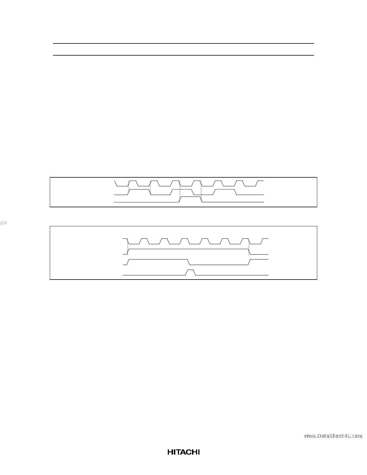
1. Generation of Signals CL1 and FLM: Signal CL1 shifts the scanning signal of the common driver. It
is a 50% duty-ratio clock that changes level synchronously with the rising edge of oscillator clock
CR.
FLM is a clock signal that is output once every 240 CL1 clock cycles for a duty of 1/240 (DUTY =
VCC), and every 120 CL1 clock cycles for a duty of 1/120 (DUTY = GND).
2. Generation of Signal M: Signal M alternates current in the LCD. It alternates the current to decrease
cross talk after a certain number of lines ranging from 2 to 63 lines. The number of lines can be
specified with pins MWS0 to MWS5 by setting each pin to either VCC or GND (H or L). In addition,
when pin MEOR is connected to GND, signal M is a simple line alternating waveform, and when pin
MEOR is connected to VCC, signal M is an EOR (exclusive OR) of line alternating waveform and
frame alternating waveform.
CR
CL1
FLM
240
(120)
1
2
Figure 6 Generation of Signals CL1 and FLM
(When MWS0 to MWS5 = 6)
CL1 DataSheet4U.com
1 2 3 4 5 6 12
M
(MEOR = GND)
M
(MEOR = VCC)
FLM
Figure 7 Generation of Signal M
DataShee
DataSheet4U.com
DataSheet4 U .com
DataSheet4U.com
937
11 Page | ||
| Páginas | Total 27 Páginas | |
| PDF Descargar | [ Datasheet HD66503.PDF ] | |
Hoja de datos destacado
| Número de pieza | Descripción | Fabricantes |
| HD66503 | 240-Channel Common Driver with Internal LCD Timing Circuit | Hitachi Semiconductor |
| Número de pieza | Descripción | Fabricantes |
| SLA6805M | High Voltage 3 phase Motor Driver IC. |
Sanken |
| SDC1742 | 12- and 14-Bit Hybrid Synchro / Resolver-to-Digital Converters. |
Analog Devices |
|
DataSheet.es es una pagina web que funciona como un repositorio de manuales o hoja de datos de muchos de los productos más populares, |
| DataSheet.es | 2020 | Privacy Policy | Contacto | Buscar |
