|
|
PDF IR2113C Data sheet ( Hoja de datos )
| Número de pieza | IR2113C | |
| Descripción | (IR2110C / IR2113C) High and Low Side Driver in Die Wafer Form | |
| Fabricantes | International Rectifier | |
| Logotipo |  |
|
Hay una vista previa y un enlace de descarga de IR2113C (archivo pdf) en la parte inferior de esta página. Total 18 Páginas | ||
|
No Preview Available !
www.DataSheet4U.com
Data Sheet No. PD65001
IR2110C/IR2113C
HIGH AND LOW SIDE DRIVER IN DIE WAFER FORM
Features
•
•
100 % Tested at Probec
Available in Chip Pack, Unsawn
Wafer,
Sawn
on
Film
d
• Floating channel designed for bootstrap operation
Fully operational to +500V or +600V
Tolerant to negative transient voltage
dV/dt immune
• Gate drive supply range from 10 to 20V
• Undervoltage lockout for both channels
• 3.3V logic compatible
Separate logic supply range from 3.3V to 20V
Logic and power ground ±5V offset
• CMOS Schmitt-triggered inputs with pull-down
• Cycle by cycle edge-triggered shutdown logic
• Matched propagation delay for both channels
• Outputs in phase with inputs
Typical Connection
up to 500V or 600V
VDD
HIN
SD
LIN
VSS
VCC
HO
VDD
VB
HIN VS
SD
LIN VCC
VSS COM
LO
TO
LOAD
(Refer to the Die Outlines for correct pin configuration). This/These diagram(s) show electrical
connections only. Please refer to our Application Notes and DesignTips for proper circuit board layout.
Note:
c This IR product is100% tested at wafer level and is manufactured using established, mature and well characterized
processes. Due to restrictions in die level processing, die may not be equivalent to standard package products and are
therefore offered with a conditional performance guarantee.The above data sheet is based on IR sample testing under
certain predetermined and assumed conditions, and are provided for illustration purposes only. Customers are encouraged
to perform testing in actual proposed packaged and use conditions. IR die products are tested using IR-based quality
assurance procedures and are manufactured using IR’s established processes. Programs for customer-specified testing
are available upon request. IR has experienced assembly yields of generally 95% or greater for individual die; however,
customer’s results will vary. Estimates such as those described and set forth in this data sheet for semiconductor die will
vary depending on a number of packaging, handling, use and other factors. Sold die may not perform on an equivalent
basis to standard package products and are therefore offered with a limited warranty as described in IR’s applicable
standard terms and conditions of sale. All IR die sales are subject to IR’s applicable standard terms and conditions of sale,
which are available upon request. For customers requiring a particular parameter to be guaranteed, special testing can be
carried out or product can be purchased as known good die.
d Part number shown is for die in wafer. Contact factory for these other options.
www.irf.com
1
DataSheet4 U .com
www.DataSheet4U.com
www.DataSheet4U.com
1 page 
www.DataSheet4U.com
IR2110C/IR2113C
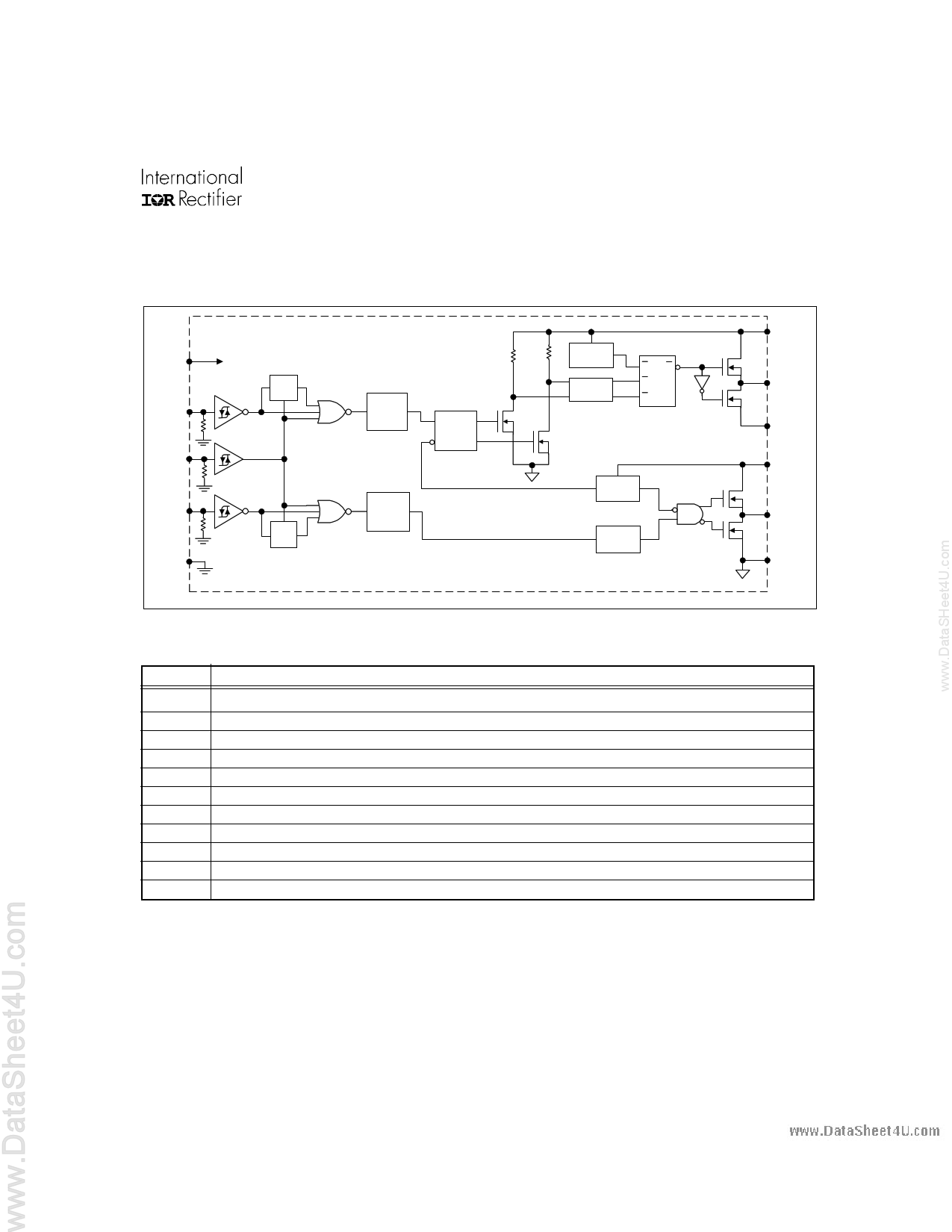
Functional Block Diagram
VDD
HIN
SD
RQ
S
VDD /VCC
LEVEL
SHIFT
PULSE
GEN
HV
LEVEL
SHIFT
UV
DETECT
PULSE
FILTER
RQ
R
S
VDD /VCC
LIN LEVEL
S
RQ
SHIFT
UV
DETECT
DELAY
VSS
Bonding Pad Definitions
Symbol Description
VDD
HIN
SD
LIN
VSS
VB
HO
VS
VCC
LO
COM
Logic supply
Logic input for high side gate driver output (HO), in phase
Logic input for shutdown
Logic input for low side gate driver output (LO), in phase
Logic ground
High side floating supply
High side gate drive output
High side floating supply return
Low side supply
Low side gate drive output
Low side return
VB
HO
VS
VCC
LO
COM
www.irf.com
DataSheet4 U .com
www.DataSheet4U.com
5
www.DataSheet4U.com
5 Page 
www.DataSheet4U.com
IR2110C/IR2113C
250 250
200
150
100
Max.
Typ.
50
200
Max.
150
Typ.
100
50
0
-50
-25
0 25 50 75
Temperature (°C)
100 125
Figure 9A. Shutdown Time vs. Temperature
250
200
Max.
150
100
Typ
50
0
0 2 4 6 8 10 12 14 16 18 20
VDD Supply Voltage (V)
Figure 9C. Shutdown Time vs. VDD Supply Voltage
0
10 12 14 16 18 20
VCC/VBS Supply Voltage (V)
Figure 9B. Shutdown Time vs. VCC/VBS Supply Voltage
100
80
60
40
M ax.
Typ.
20
0
-50
-25
0 25 50 75
Temperature (°C)
100 125
Figure 10A. Turn-On Rise Time vs. Temperature
100 50
80 40
60
Max.
40
Typ.
20
30
Max.
20
Typ.
10
0
10
12 14 16 18
VBIAS Supply Voltage (V)
Figure 10B. Turn-On Rise Time vs. Voltage
20
0
-50
-25
0 25 50 75
Temperature (°C)
100 125
Figure 11A. Turn-Off Fall Time vs. Temperature
www.irf.com
11
DataSheet4 U .com
www.DataSheet4U.com
www.DataSheet4U.com
11 Page | ||
| Páginas | Total 18 Páginas | |
| PDF Descargar | [ Datasheet IR2113C.PDF ] | |
Hoja de datos destacado
| Número de pieza | Descripción | Fabricantes |
| IR2113 | HIGH AND LOW SIDE DRIVER | International Rectifier |
| IR2113C | (IR2110C / IR2113C) High and Low Side Driver in Die Wafer Form | International Rectifier |
| IR2113PBF | HIGH AND LOW SIDE DRIVER | International Rectifier |
| IR2113S | HIGH AND LOW SIDE DRIVER | International Rectifier |
| Número de pieza | Descripción | Fabricantes |
| SLA6805M | High Voltage 3 phase Motor Driver IC. |
Sanken |
| SDC1742 | 12- and 14-Bit Hybrid Synchro / Resolver-to-Digital Converters. |
Analog Devices |
|
DataSheet.es es una pagina web que funciona como un repositorio de manuales o hoja de datos de muchos de los productos más populares, |
| DataSheet.es | 2020 | Privacy Policy | Contacto | Buscar |
