|
|
PDF IR3637SPBF Data sheet ( Hoja de datos )
| Número de pieza | IR3637SPBF | |
| Descripción | 1% ACCURATE SYNCHRONOUS PWM CONTROLLER | |
| Fabricantes | International Rectifier | |
| Logotipo |  |
|
Hay una vista previa y un enlace de descarga de IR3637SPBF (archivo pdf) en la parte inferior de esta página. Total 21 Páginas | ||
|
No Preview Available !
www.DataSheet4U.com
Data Sheet No. PD94713
IR3637SPBF
1% ACCURATE SYNCHRONOUS PWM CONTROLLER
FEATURES
0.8V Reference Voltage
Operates with a single 5V Supply Voltage
Internal 400kHz Oscillator
Soft-Start Function
Fixed Frequency Voltage Mode
Short Circuit Protection
APPLICATIONS
Computer Peripheral Voltage Regulator
Memory Power supplies
Graphics Card
Low cost on-board DC to DC
DESCRIPTION
The IR3637 controller IC is designed to provide a simple
synchronous Buck regulator for on-board DC to DC ap-
plications in a small 8-pin SOIC. The output voltage can
be precisely regulated using the internal 0.8V reference
voltage for low voltage applications.
The IR3637 operates at a fixed internal 400kHz switch-
ing frequency to reduce the component size.
The device features under-voltage lockout for both input
supplies, an external programmable soft-start function
as well as output under-voltage detection that latches
off the device when an output short is detected.
TYPICAL APPLICATION
12V
C3
5V
C2
C1
Vc Vcc
HDrv
Q1
L1
SS/SD
D1
C4
IR3637 LDrv
Q2
Comp
C5
Fb
Gnd
R1
R3
R2
Vout
C6
Figure 1 - Typical application of IR3637.
ORDERING INFORMATION
PKG
DESIG
S
S
PACKAGE PIN PARTS PARTS T & R
DESCRIPTION COUNT PER TUBE PER REEL Oriantation
IR3637SPBF
IR3637STRPBF
8
8
95
-------
------
2500
Fig A
Rev. 1.1
06/16/05
www.irf.com
1
1 page 
www.DataSheet4U.com
IR3637SPBF
THEORY OF OPERATION
Soft-Start
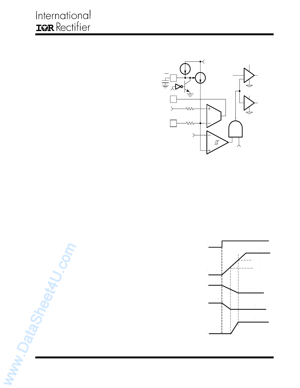
The IR3637 has a programmable soft-start to control the
output voltage rise and limit the current surge at the start-
up. To ensure correct start-up, the soft-start sequence
initiates when the Vc and Vcc rise above their threshold
(3.3V and 4.2V respectively) and generates the Power
On Reset (POR) signal. Soft-start function operates by
sourcing an internal current to charge an external ca-
pacitor to about 3V. Initially, the soft-start function clamps
the E/A’s output of the PWM converter and disables the
short circuit protection. During the power up, the output
starts at zero and voltage at Fb is below 0.4V. The feed-
back UVLO is disabled during this time by injecting a
current (64µA) into the Fb. This generates a voltage
about 1.6V (64µA×25K) across the negative input of E/
A and positive input of the feedback UVLO comparator
(see Figure 3).
The magnitude of this current is inversely proportional to
the voltage at soft-start pin.
25uA
SS/SD
3V
64uA
Max
HDrv
POR
Comp
0.8V
Fb
25K
25K
Error Amp
LDrv
0.4V
64uA×25K=1.6V
When SS=0
POR
Feeback
UVLO Comp
Figure 3 - Soft-start circuit for IR3637.
The 20µA current source starts to charge up the exter-
nal capacitor. In the mean time, the soft-start voltage
ramps up, the current flowing into Fb pin starts to de-
crease linearly and so does the voltage at the positive
pin of feedback UVLO comparator and the voltage nega-
tive input of E/A.
The output start-up time is the time period when soft-
start capacitor voltage increases from 1V to 2V. The start-
up time will be dependent on the size of the external
soft-start capacitor. The start-up time can be estimated
by:
25µA×TSTART/CSS = 2V-1V
When the soft-start capacitor is around 1V, the current
flowing into the Fb pin is approximately 32µA. The volt-
age at the positive input of the E/A is approximately:
For a given start up time, the soft-start capacitor can be
estimated as:
CSS ≅ 25µA×TSTART/1V
32µA×25K = 0.8V
The E/A will start to operate and the output voltage starts
to increase. As the soft-start capacitor voltage contin-
ues to go up, the current flowing into the Fb pin will keep
decreasing. Because the voltage at pin of E/A is regu-
lated to reference voltage 0.8V, the voltage at the Fb is:
VFB = 0.8-25K×(Injected Current)
The feedback voltage increases linearly as the injecting
current goes down. The injecting current drops to zero
when soft-start voltage is around 2V and the output volt-
age goes into steady state.
As shown in Figure 4, the positive pin of feedback UVLO
comparator is always higher than 0.4V, therefore, feed-
back UVLO is not functional during soft-start.
Output of UVLO
POR
3V
Soft-Start 0V
Voltage
64uA
Current flowing
into Fb pin
Voltage at negative input ≅1.6V
of Error Amp and Feedback
UVLO comparator
≅2V
≅1V
0uA
0.8V
0.8V
0V
Voltage at Fb pin
Figure 4 - Theoretical operational waveforms
during soft-start.
Rev. 1.1
06/16/05
www.irf.com
5
5 Page 
www.DataSheet4U.com
IR3637SPBF
6) Place second pole at the ESR zero.
FP2 = FESR
R8 =
1
2π × C10 × FP2
1
Check if R8 > gm
If R8 is too small, increase R7 and start from step 2.
7) Place second zero around the resonant frequency.
FZ2 = FLC
R6
=
2π ×
1
C10 × FZ2
-
R8
8) Use equation (1) to calculate R5.
R5
=
VREF
VOUT - VREF
×
R6
These design rules will give a crossover frequency ap-
proximately one-tenth of the switching frequency. The
higher the band width, the potentially faster the load tran-
sient speed. The gain margin will be large enough to
provide high DC-regulation accuracy (typically -5dB to -
12dB). The phase margin should be greater than 45 for
overall stability.
Layout Consideration
The layout is very important when designing high fre-
quency switching converters. Layout will affect noise
pickup and can cause a good design to perform with
less than expected results.
Start to place the power components, make all the con-
nection in the top layer with wide, copper filled areas.
The inductor, output capacitor and the MOSFET should
be close to each other as possible. This helps to reduce
the EMI radiated by the power traces due to the high
switching currents through them. Place input capacitor
directly to the drain of the high-side MOSFET, to reduce
the ESR replace the single input capacitor with two par-
allel units. The feedback part of the system should be
kept away from the inductor and other noise sources,
and be placed close to the IC. In multilayer PCB use
one layer as power ground plane and have a control cir-
cuit ground (analog ground), to which all signals are ref-
erenced. The goal is to localize the high current path to
a separate loop that does not interfere with the more
sensitive analog control function. These two grounds
must be connected together on the PC board layout at a
single point.
Based on the frequency of the zero generated by ESR
versus crossover frequency, the compensation type can
be different. The table below shows the compensation
type and location of crossover frequency.
Compensator Location of Zero
Type Crossover Frequency
(FO)
Type II (PI)
FLC < FESR < FO < fS/2
Type III (PID)
Method A
Type III (PID)
Method B
FLC < FO < FESR < fS/2
FLC < FO < fS/2 < FESR
Typical
Output
Capacitor
Electrolytic,
Tantalum
Tantalum,
Ceramic
Ceramic
Table - The compensation type and location of zero
crossover frequency.
Detail information is dicussed in application Note AN-
1043 which can be downloaded from the IR Web-Site.
All design should be tested for stability to verify the cal-
culated values.
Rev. 1.1
06/16/05
www.irf.com
11
11 Page | ||
| Páginas | Total 21 Páginas | |
| PDF Descargar | [ Datasheet IR3637SPBF.PDF ] | |
Hoja de datos destacado
| Número de pieza | Descripción | Fabricantes |
| IR3637SPBF | 1% ACCURATE SYNCHRONOUS PWM CONTROLLER | International Rectifier |
| Número de pieza | Descripción | Fabricantes |
| SLA6805M | High Voltage 3 phase Motor Driver IC. |
Sanken |
| SDC1742 | 12- and 14-Bit Hybrid Synchro / Resolver-to-Digital Converters. |
Analog Devices |
|
DataSheet.es es una pagina web que funciona como un repositorio de manuales o hoja de datos de muchos de los productos más populares, |
| DataSheet.es | 2020 | Privacy Policy | Contacto | Buscar |
