|
|
|
PDF MT9V022I77ATC Data sheet ( Hoja de datos )
| Número de pieza | MT9V022I77ATC | |
| Descripción | (MT9V022I77ATM / MT9V022I77ATC) Wide VGA CMOS Digital Image Sensor | |
| Fabricantes | Micron Technology | |
| Logotipo | ||
Hay una vista previa y un enlace de descarga de MT9V022I77ATC (archivo pdf) en la parte inferior de esta página. Total 15 Páginas | ||
|
No Preview Available !
www.DataSheet4U.com
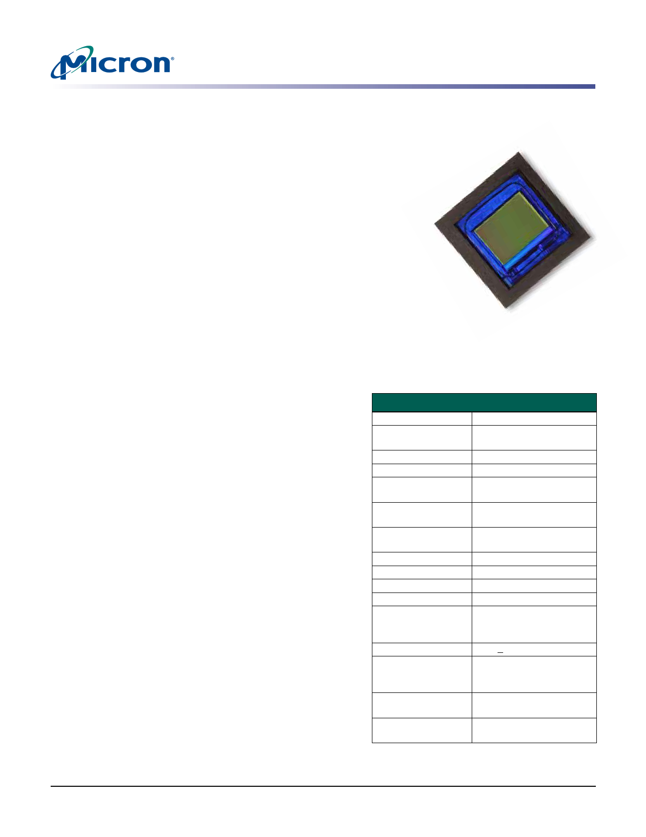
MT9V022I77ATM (mono)
MT9V022I77ATC (color)
1/3-Inch, Wide-VGA CMOS Digital Image Sensor
Rugged Specs and High Quality for Scene-Understanding
and Smart Imaging Applications Micron’s MT9V022 has specifi-
cally been designed to support the demanding interior and exterior
needs of automotive imaging, which makes it ideal for a wide vari-
ety of scene understanding and smart imaging applications in real-
world environments. This wide-VGA CMOS image sensor features
DigitalClarity™, Micron’s breakthrough, low-noise CMOS imaging
technology that achieves CCD image quality (based on signal-to-
noise ratio and low-light sensitivity) while maintaining the inher-
ent size, cost, and integration advantages of CMOS.
Applications
• Automotive
• Unattended surveillance
• Stereo vision
• Security
• Smart vision
• Automation
• Video as input
• Machine vision
Features
• Micron’s DigitalClarity™
•
CMOS imaging technology
• Double-buffered global shutter
photodiode pixels
•
• Simultaneous integration and
readout
• Enhanced Near-IR
performance (NIR QE >35%) •
• Progressive or interlaced
readout modes
• Linear or high dynamic range
pixel response
•
• >99% global shutter efficiency •
• Register lock capability
• User-Programmable window
size within frame
• 2 x 2 and 4 x 4 pixel averaging
of the full resolution
• ADC On-Chip (10-bit linear or
12-bit to 10-bit companding
• wmAwuotdowee).xDpoastuareSchoneterotl4(AUEC.c)om
• Auto gain control (AGC)
• Black level calibration (BLC)
User-Programmable regional
gain and exposure weighting
(25 regions)
Support for 4 unique serial
control register IDs to control
multiple imagers on the same
bus
Master/Slave dual sensor
operation for stereoscopic,
foveal, or hyperspectral
operation
On-Chip digital thermometer
Data output formats:
– Single sensor mode: 10-bit
parallel/stand-alone or 8-
bit or 10-bit serial LVDS
– Dual sensor mode:
Interspersed 8-bit serial
LVDS
Key Parameters
Optical format
Active imager size
Active pixels
Pixel size
Color filter array
Shutter type
Maximum data rate
Master clock
Full resolution
Frame rate
ADC resolution
Responsivity
Dynamic range
Supply voltage
Power consumption
Operating
temperature
Packaging
1/3-inch
4.51mm(H) x 2.88mm(V)
5.35mm Diagonal
752H x 480V
6.0µm x 6.0µm
Monochrome or color RGB
Bayer pattern
Double-Buffered global
shutter TrueSNAP™
26.6 Mp/s
26.6 MHz
752 x 480
60 fps (at full resolution)
10-bit
4.8 V/lux-sec (550nm)
>55dB linear;
>80dB–100dB in HiDy
Mode
3.3V +0.3V (all supplies)
<320mW at maximum
data rate; 100µW standby
current
–40°C to +85°C
52-ball IBGA, automotive-
qualified; wafer or die
Micron Technology, Inc., reserves the right to change products or specifications without notice.
©2006 Micron Technology, Inc. All rights reserved.
Products and specifications discussed herein are subject to change by Micron without notice.
1 page 
www.DataSheet4U.com
MT9V022: 1/3-Inch Wide-VGA Digital Image Sensor
Output Data Timing
Output Data Timing
The data output of the MT9V022 is synchronized with the PIXCLK output. When
LINE_VALID is HIGH, one 10-bit pixel datum is output every PIXCLK period.
Figure 5: Row Timing and FRAME_VALID/LINE_VALID Signals
FRAME_VALID
LINE_VALID
Number of master clocks
P1 A
Q
...
...
...
AQ
A P2
Figure 6: Timing Example of Pixel Data
LINE_VALID
....
PIXCLK
....
Blanking
Valid Image Data
....
DOUT(9:0)
P0
(9:0)
P1
(9:0)
P2
(9:0)
P3
(9:0)
P4
(9:0)
....
Pn-1
(9:0)
Note: The parameters P1, A, Q, and P2 are defined in Table 1 on page 5.
Table 1: Frame Time
Parameter
A
P1
P2
Q
A+Q
V
Nrows
F
Description
Active data time
Frame start blanking
Frame end blanking
Horizontal blanking
Row time
Vertical blanking
Frame valid time
Total frame time
Pixel Clock
752
71
23
94
846
38,074
406,080
444,154
Master Clocks
752
71
23
94
846
38,074
406,080
444,154
Time
28.02
2.66
0.86
3.52
31.72
1.43
15.23
16.66
Blanking
Pn
(9:0)
Units
µs
µs
µs
µs
µs
ms
ms
ms
Serial Bus Description
The MT9V022 control registers are written to and read from the two-wire serial interface
bus. The MT9V022 is a serial interface slave with four possible IDs (0x90, 0x98, 0xB0, and
0xB8) determined by S_CTRL_ADR0 and S_CTRL_ADR1 inputs.
Data is transferred into the MT9V022 and out through the serial data (SDATA) line. The
SDATA line is pulled up to VDD off-chip by a 1. 5kΩ resistor. Either the slave or master
device can pull the SDATA line down. The serial interface protocol determines which
device is allowed to pull the SDATA line down at any given time.
Register Lock
A register lock feature is included in the MT9V022 to help reduce the probability of an
inadvertent, noise-triggered two-wire serial interface WRITE to the sensor. The user may
www.DataSheet4U.loccokmall registers or only the read mode register. The read mode register controls the
image orientation, and an unintended flip to the image can cause serious results.
PDF:09005aef8201ffc3/Source: 09005aef81ff2525
MT9V022_Product_Brief - Rev. A 1/06 EN
5 Micron Technology, Inc., reserves the right to change products or specifications without notice.
©2006 Micron Technology, Inc. All rights reserved.
5 Page 
www.DataSheet4U.com
MT9V022: 1/3-Inch Wide-VGA Digital Image Sensor
Electrical Specifications
Figure 12: Quantum Efficiency – Color and Monochrome
60 Blue
Green (B)
Green (R)
Red
50 MONO
40
30
20
10
0
350 450 550 650 750 850 950 1,050
Wavelength (nm)
Figure 13: Typical Configuration (Connection) – Parallel Output Mode
VDD
VAA VAAPIX
Master Clock
STANDBY from
Controller or
Digital GND
Two-Wire
Serial Interface
VDDLVDS VDD
SYSCLK
OE
RESET#
EXPOSURE
STANDBY
S_CTRL_ADR0
S_CTRL_ADR1
SCLK
SDATA
VAA VAAPIX
DOUT(9:0)
LINE_VALID
FRAME_VALID
PIXCLK
LED_OUT
ERROR
To Controller
To LED output
0.1μF
RSVD
DGND LVDSGND
AGND
Note: LVDS signals are to be left floating.
www.DataSheet4U.com
PDF:09005aef8201ffc3/Source: 09005aef81ff2525
MT9V022_Product_Brief - Rev. A 1/06 EN
11
Micron Technology, Inc., reserves the right to change products or specifications without notice.
©2006 Micron Technology, Inc. All rights reserved.
11 Page | ||
| Páginas | Total 15 Páginas | |
| PDF Descargar | [ Datasheet MT9V022I77ATC.PDF ] | |
Hoja de datos destacado
| Número de pieza | Descripción | Fabricantes |
| MT9V022I77ATC | (MT9V022I77ATM / MT9V022I77ATC) Wide VGA CMOS Digital Image Sensor | Micron Technology |
| MT9V022I77ATM | (MT9V022I77ATM / MT9V022I77ATC) Wide VGA CMOS Digital Image Sensor | Micron Technology |
| Número de pieza | Descripción | Fabricantes |
| SLA6805M | High Voltage 3 phase Motor Driver IC. |
Sanken |
| SDC1742 | 12- and 14-Bit Hybrid Synchro / Resolver-to-Digital Converters. |
Analog Devices |
|
DataSheet.es es una pagina web que funciona como un repositorio de manuales o hoja de datos de muchos de los productos más populares, |
| DataSheet.es | 2020 | Privacy Policy | Contacto | Buscar |