|
|
PDF STA014T Data sheet ( Hoja de datos )
| Número de pieza | STA014T | |
| Descripción | (STA014x) MPEG 2.5 LAYER III AUDIO DECODER WITH ADPCM AND SRS WOWO POSTPROCESSING CAPABILITY | |
| Fabricantes | ST Microelectronics | |
| Logotipo |  |
|
Hay una vista previa y un enlace de descarga de STA014T (archivo pdf) en la parte inferior de esta página. Total 30 Páginas | ||
|
No Preview Available !
® STA014 STA014B STA014T
MPEG
2.5
LSARYESRWIIOI WAU®DPIOOSDTEPCROODCEERSWSIINTGH
ADPCM AND
CAPABILITY
PRODUCT PREVIEW
The Device incorporates the SRS
WOW® Technology under li-
cence from SRS Labs, Inc.
mSINGLE CHIP MPEG2 LAYER 3 DECODER
SUPPORTING:
o- All features specified for Layer III in ISO/IEC
11172-3 (MPEG 1 Audio)
.c- All features specified for Layer III in ISO/IEC
13818-3.2 (MPEG 2 Audio)
- Lower sampling frequencies syntax extension,
U(not specified by ISO) called MPEG 2.5
DECODES LAYER III STEREO CHANNELS,
t4DUAL CHANNEL, SINGLE CHANNEL
(MONO)
eSUPPORTING ALL THE MPEG 1 & 2 SAM-
PLING FREQUENCIES AND THE EXTEN-
eSION TO MPEG 2.5:
48, 44.1, 32, 24, 22.05, 16, 12, 11. 025, 8 KHz
hACCEPTS MPEG 2.5 LAYER III ELEMEN-
TARY COMPRESSED BITSTREAM WITH
SDATA RATE FROM 8 Kbit/s UP TO 320 Kbit/s
ADPCM CODEC CAPABILITIES:
ta- sample frequencyfrom 8 kHz to 32 kHz
- sample size from 8 bits to 32 bits
a- encodingalgorithm: DVI,
ITU-G726pack (G723-24,G721,G723-40)
- Tone controlandfast-forward capability
.DSRS WOW(1) TECHNOLOGY CAN BE USED
AS POSTPROCESSING. SUPPORT FOR
DIFFERENT SPEAKERS TYPES:
w- headphone
- medium
w- large
WOW(1) TRUEBASS AND FOCUS CAN BE
wINDIPENDENTLY ADJUSTED
EASY PROGRAMMABLE GPSO INTERFACE
mFOR ENCODED DATA UP TO 5Mbit/s
o(TQFP44 & LFBGA 64)
.cDIGITAL VOLUME
UBASS & TREBLE CONTROL
t4SERIAL BITSTREAM INPUT INTERFACE
eEASYPROGRAMMABLE ADC INPUT INTERFACE
eANCILLARY DATA EXTRACTION VIA I2C IN-
hTERFACE.
SSERIAL PCM OUTPUT INTERFACE (I2S
ataAND OTHER FORMATS)
ORDERING NUMBERS: STA014 (SO28)
STA014T (TQFP44)
STA014B (LFBGA 64)
PLL FOR INTERNAL CLOCK AND FOR OUT-
PUT PCM CLOCK GENERATION
CRC CHECK AND SYNCHRONISATION ER-
ROR DETECTION WITH SOFTWARE INDI-
CATORS
I2C CONTROL BUS
LOW POWER 2.4V CMOS TECHNOLOGY
WIDE RANGE OF EXTERNAL CRYSTALS
FREQUENCIES SUPPORTED
APPLICATIONS
PC SOUND CARDS
MULTIMEDIA PLAYERS
VOICE RECORDERS
DESCRIPTION
The STA014 is a fully integrated high flexibility
MPEG Layer III Audio Decoder, capable of de-
coding Layer III compressed elementary streams,
as specified in MPEG 1 and MPEG 2 ISO stand-
ards. The device decodes also elementarystreams
compressed by using low sampling rates, as speci-
fied by MPEG 2.5. STA014 receives the input data
through a Serial Input Interface. The decoded sig-
nal is a stereo, mono, or dual channel digital output
that can be sent directly to a D/A converter, by the
PCM Output Interface. This interface is software
programmable to adapt the STA014 digital output
to the most common DACs architectures used on
the market. The functional STA014 chip partitioning
is described in Fig.1a and Fig.1b.
w.DJuly 2000
1/45
wThis is preliminary information on a new product now in development or undergoing evaluation. Details are subject to change without notice.
w(1) in order to enable SRS WOW algorithm a mandatory configuration fil e is required.
1 page 
STA014-STA014B-STA014T
PIN DESCRIPTION
SO28 TQFP44 LFBGA64
1 29
B5
2 30
B4
3 31
A4
Pin Name
VDD_1
VSS_1
SDA
Type
I/O
4 32
5 34
6 36
7 38
B3
A1
B2
D4
SCL
SDI
SCKR
BIT_EN
I
I
I
I
8 40
D1 SRC_INT/SCK_ADC I
9 42
10 44
11 2
12 3
E2
F2
H1
H3
SDO
SCKT
LRCLKT
OCLK
O
O
O
I/O
13 5
14 6
15 7
16 8
17 10
18 11
19 12
F3
E4
G4
G5
F5
G6
G7
VSS_2
VDD_2
VSS_3
VDD_3
PVDD
PVSS
FILT
O
20 13
21 15
G8
F7
XTO
XTI
O
I
22 19
23 21
24 22
E7
C8
D7
VSS_4
VDD_4
TESTEN
I
25 24
26 25
A7
B6
SDI_ADC
RESET
I
I
27 26
A5
LRCK_ADC
I
28 27
C5
OUT_CLK/
DATA_REQ
O
20 C7
IODATA[0]
I/O
18 E6
IODATA[1]
I/O
16 F6
IODATA[2]
I/O
14 F8
IODATA[3]
I/O
37 C3
IODATA[4]
I/O
39 E3
IODATA[5]
I/O
41 D2
IODATA[6]
I/O
43 F1
IODATA[7]
I/O
35 C2 GPIO_STROBE I/O
4 G3
GPSO_REQ
O
28 C6
GPSO_SCKR
I
33 A2
GPSO_DATA
O
Note: In functional mode TESTEN must be connected to VDD.
Function
Supply Voltage
Ground
i2C Serial Data +
Acknowledge
I2C Serial Clock
Receiver Serial Data
Receiver Serial Clock
Bit Enable
Interrupt Line/ADC Serial
Clock
TransmitterSerial Data(PCM Data)
Transmitter Serial Clock
Transmitter Left/Right Clock
Oversampling Clock for DAC
Ground
Supply Voltage
Ground
Supply Voltage
PLL Power
PLL Ground
PLL Filter Ext. Capacitor
Conn.
Crystal Output
Crystal Input (Clock Input)
Ground
Supply Voltage
Test Enable
ADC Data Input
System Reset
ADC Left/Right Clock
Buffered Output Clock/
Data Request Signal
GPIO Data Line
GPIO Data Line
GPIO Data Line
GPIO Data Line
GPIO Data Line
GPIO Data Line
GPIO Data Line
GPIO Data Line
GPIO Strobe Signal
GPSO Request Signal
GPSO Serial Clock
GPSO Serial Data
PAD Description
CMOS Input Pad Buffer
CMOS 4mA Output Drive
CMOS Input Pad Buffer
CMOS Input Pad Buffer
CMOS Input Pad Buffer
CMOS Input Pad Buffer with
pull up
CMOS Input Pad Buffer
CMOS 4mA Output Drive
CMOS 4mA Output Drive
CMOS 4mA Output Drive
CMOS Input Pad Buffer
CMOS 4mA Output Drive
CMOS 4mA Output Drive
Specific Level Input Pad
(see paragraph 2.1)
CMOS Input Pad Buffer with
pull up
CMOS Input Pad Buffer
CMOS Input Pad Buffer with
pull up
CMOS Output Pad Buffer
CMOS 4mA Output Drive
CMOS 4mA Schmitt Trigger
Bidir Pad Buffer
CMOS Output Pad Buffer
CMOS Input Pad Buffer
CMOS Output Pad Buffer
5/45
5 Page 
STA014-STA014B-STA014T
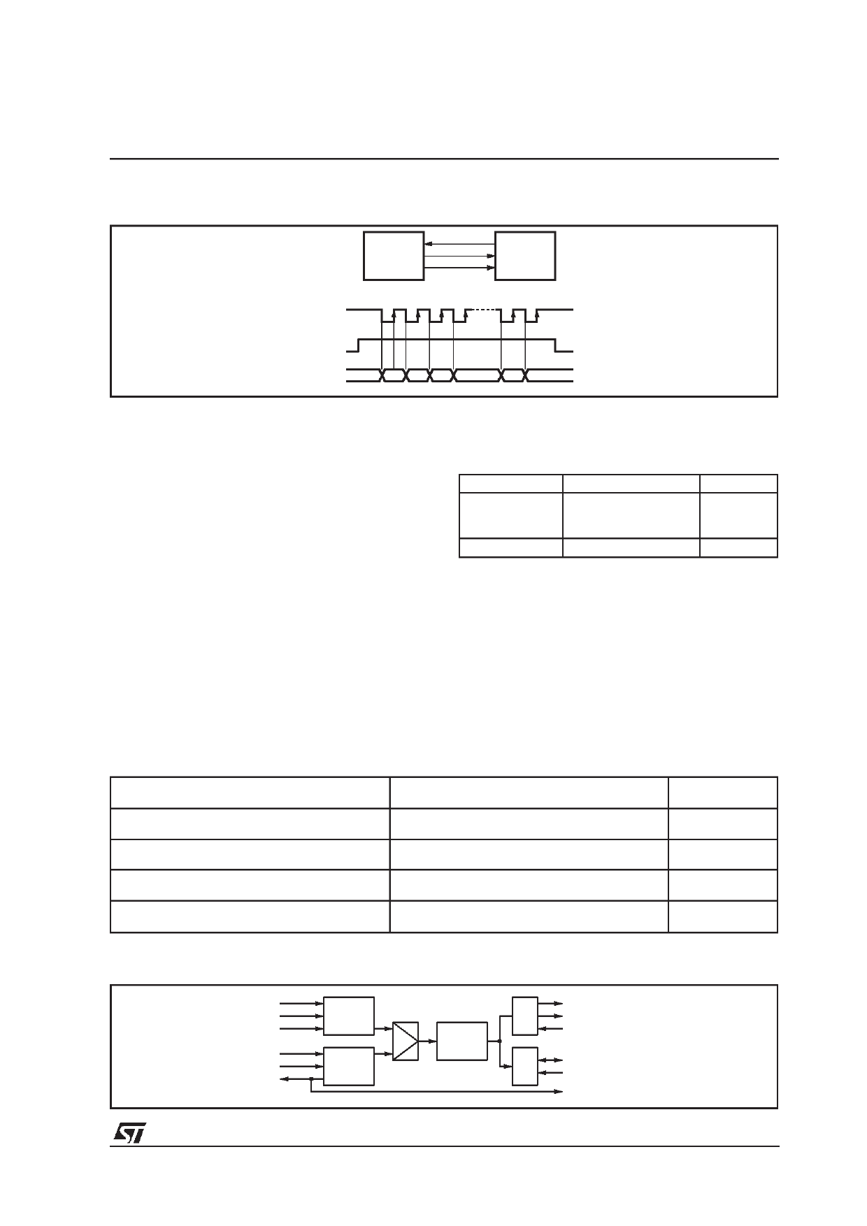
Figure 10.
GPSO_SCKR
GPSO_DATA
GPSO_REQ
MCU
GPSO_SCKR
GPSO_REQ
GPSO_DATA
To enable the GPSO interface bit GEN of
GPSO_ENABLE register must be set. Using the
GPSO_CONF register the protocol can be config-
ured in order to provide outcoming data on ris-
ing/falling edge of GPSO_SCKR input clock; the
GPSO_REQ request signal polarity (usually con-
nected to an MCU interrupt line) can be config-
ured as well.
3.4 ADC Inteface
Beside the serial input interface based on SDI
and SCKR lines a 3 wire flexible and user config-
urable input interface is also available, suitable to
interface with most A/D converters. To configure
this interface 4 specific I2C registers are available
(ADC_ENABLE, ADC_CONF, ADC_WLEN and
ADC_WPOS). Refer to registers description for
more details.
3.5 General Purpose I/O Interface
A new general purpose I/O interface has been
added to this device (TQFP44 and LFBGA64
only). Actually only the strobe line is used in
D00AU1145
ADPCM encoding mode to provide an interrupt;
other pins are reserved for future use. The re-
lated configuration register is GPIO_CONF. See
the following summary for related pin usage:
Name
I/ODATA [0]
....................
I/ODATA [7]
GPIO_STROBE
Description
GPIO data line
GPIO strobe line
Dir
I/O
....
I/O
I/O
4 ADPCM ENCODING: Overview
According to the previously described interfaces
there are 4 ways to manage ADPCM data stream
while encoding. Input interface can be either the
serial receiver block (SDI + SCKR + DATA_REQ
lines) or the ADC specific interface.
Output interfaces can be either the I2C bus (with
or without interrupt line) or the GPSO high-speed
serial interface (GPSO_REQ + GPSO_ DATA +
GPSO_SCKR lines). This result in the following 4
methods to handle encoding flow:
INPUT (data to encode)
Output (encoded data)
ADC I/F (SDI_ADC + LRCK_ADC + SCK_ADC) GPSO I/F (GPSO_REQ + GPSO_DATA +
GPSO_SCKR)
ADC I/F (SDI_ADC + LRCK_ADC + SCK_ADC) I2C + Interrupt (SCL + SDA + DATA_REQ)
SERIAL I/F (SCKR + SDI + DATA_REQ)
SERIAL I/F (SCKR + SDI + DATA_REQ) (*)
GPSO I/F (GPSO_REQ + GPSO_DATA +
GPSO_SCKR)
I2C (polling) (SCL + SDA)
Available on
package
TQFP44
LFBGA64
SO28/TQFP44
LFBGA64
TQFP44
LFBGA64
SO28/TQFP44
LFBGA64
(*) STA013 Compatible mode
Figure. 11
LRCK_ADC
SDI_ADC
SCK_ADC
ADC I/F
SDI
SCKR
DATA_REQ
SERIAL
RECEIVER
MUX
ENCOD
ENGINE
GPSO
GPSO_REQ
GPSO_DATA
GPSO_SCKR
I2C
D99AU1064
SDA
SCL
DATA_REQ
11/45
11 Page | ||
| Páginas | Total 30 Páginas | |
| PDF Descargar | [ Datasheet STA014T.PDF ] | |
Hoja de datos destacado
| Número de pieza | Descripción | Fabricantes |
| STA014 | (STA014x) MPEG 2.5 LAYER III AUDIO DECODER WITH ADPCM AND SRS WOWO POSTPROCESSING CAPABILITY | ST Microelectronics |
| STA014B | (STA014x) MPEG 2.5 LAYER III AUDIO DECODER WITH ADPCM AND SRS WOWO POSTPROCESSING CAPABILITY | ST Microelectronics |
| STA014T | (STA014x) MPEG 2.5 LAYER III AUDIO DECODER WITH ADPCM AND SRS WOWO POSTPROCESSING CAPABILITY | ST Microelectronics |
| Número de pieza | Descripción | Fabricantes |
| SLA6805M | High Voltage 3 phase Motor Driver IC. |
Sanken |
| SDC1742 | 12- and 14-Bit Hybrid Synchro / Resolver-to-Digital Converters. |
Analog Devices |
|
DataSheet.es es una pagina web que funciona como un repositorio de manuales o hoja de datos de muchos de los productos más populares, |
| DataSheet.es | 2020 | Privacy Policy | Contacto | Buscar |
