|
|
|
PDF IN74AC299 Data sheet ( Hoja de datos )
| Número de pieza | IN74AC299 | |
| Descripción | 8-Bit Universal Shift/Storage Register | |
| Fabricantes | IK Semiconductor | |
| Logotipo | ||
Hay una vista previa y un enlace de descarga de IN74AC299 (archivo pdf) en la parte inferior de esta página. Total 9 Páginas | ||
|
No Preview Available !
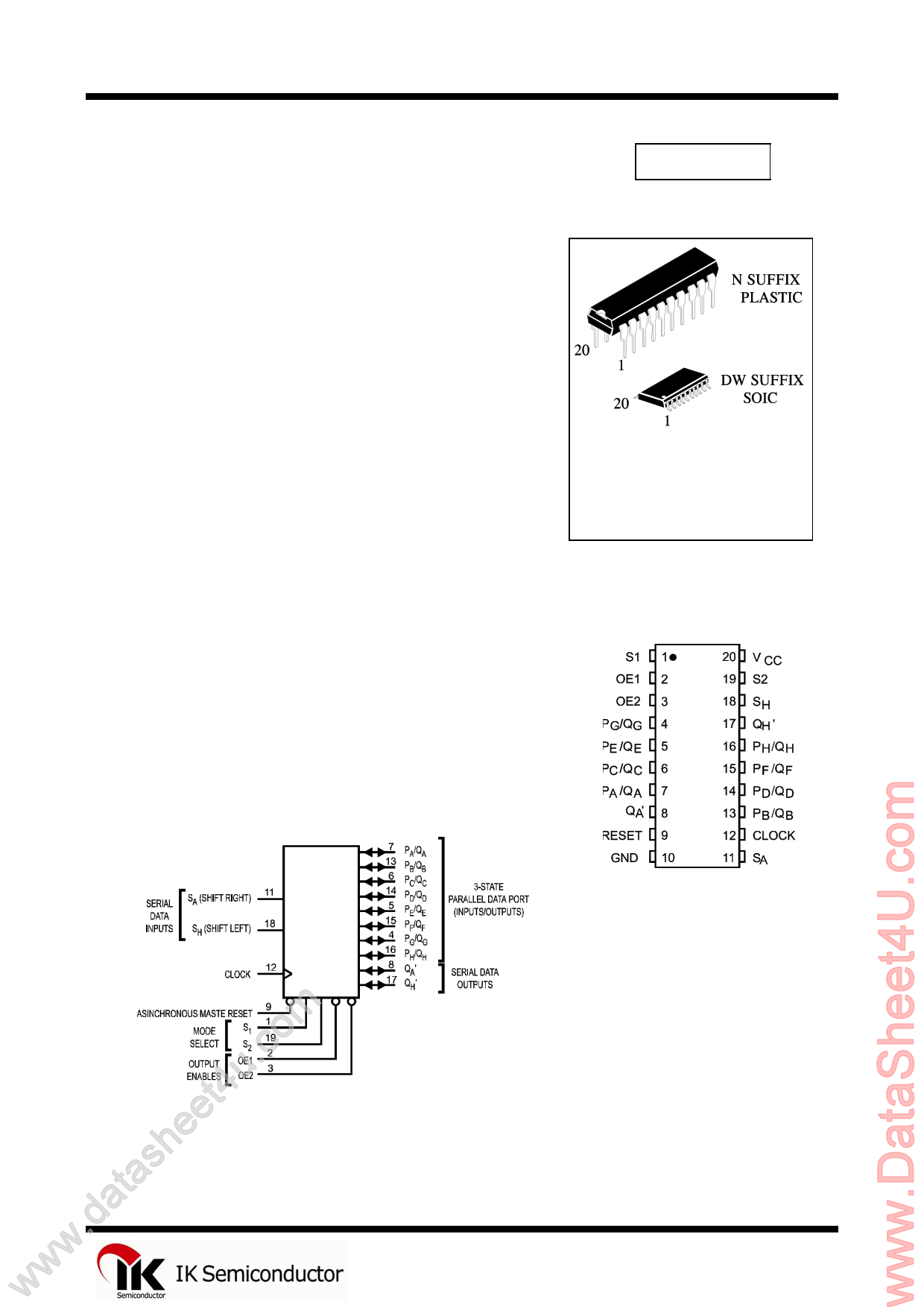
TECHNICAL DATA
8-Bit Bidirectional Universal
Shift Register with Parallel I/O
High-Speed Silicon-Gate CMOS
IN74AC299
The IN74AC299 is identical in pinout to the LS/ALS299,
HC/HCT299. The device inputs are compatible with standard CMOS
outputs; with pullup resistors, they are compatible with LS/ALS outputs.
The IN74AC299 features a multiplexed parallel input/output data port
to achieve full 8-bit handling in a 20 pin package. Due to the large output
drive capability and the 3-state feature, this device is ideally suited for
interface with bus lines in a bus-oriented system.
Two Mode-Select inputs and two Output Enable inputs are used to
choose the mode of operation as listed in the Function Table.
Synchronous parallel loading is accomplished by taking both Mode-
Select lines, S1 and S2, high. This places the outputs in the high-
impedance state, which permits data applied to the data port to be clocked
into the register. Reading out of the register can be accomplished when
the outputs are enabled. The active-low asynchronous Reset overrides all
other inputs.
• Outputs Directly Interface to CMOS, NMOS, and TTL
• Operating Voltage Range: 2.0 to 6.0 V
• Low Input Current: 1.0 µA; 0.1 µA @ 25°C
• High Noise Immunity Characteristic of CMOS Devices
• Outputs Source/Sink 24 mA
ORDERING INFORMATION
IN74AC299N Plastic
IN74AC299DW SOIC
TA = -40° to 85° C for all packages
PIN ASSIGNMENT
LOGIC DIAGRAM
www.datasheet4u.coPPImNIN1020==GVNCCD
1
1 page 
IN74AC299
TIMING REQUIREMENTS (CL=50pF,Input tr=tf=3.0 ns)
Symbol
Parameter
VCC*
V
tsu Minimum Setup Time, Mode Select S1 or S2
to Clock (Figure 4)
tsu Minimum Setup Time, Data Inputs PA thru PH
to Clock (Figure 4)
tsu Minimum Setup Time, Data Inputs SA, SH to
Clock (Figure 4)
th Minimum Hold Time, Clock to Mode Select
S1 or S2 (Figure 4)
th Minimum Hold Time, Clock to Data Inputs PA
thru PH (Figure 4)
th Minimum Hold Time, Clock to Data Inputs
SA, SH (Figure 4)
trec Minimum Recovery Time, Reset Inactive to
Clock (Figure 2)
tw Minimum Pulse Width, Clock (Figure 1)
tw Minimum Pulse Width, Reset (Figure 2)
*Voltage Range 3.3 V is 3.3 V ±0.3 V
Voltage Range 5.0 V is 5.0 V ±0.5 V
3.3
5.0
3.3
5.0
3.3
5.0
3.3
5.0
3.3
5.0
3.3
5.0
3.3
5.0
3.3
5.0
3.3
5.0
Guaranteed Limits
25 °C
-40°C to
85°C
8.0 8.5
5.0 5.5
5.5 6.0
3.5 4.0
6.5 7.0
4.0 4.5
0.5 0.5
1.0 1.0
00
1.0 1.0
0 0.5
1.0 1.0
1.5 1.5
1.5 1.5
4.5 5.0
3.5 3.5
4.5 5.0
3.5 3.5
Unit
ns
ns
ns
ns
ns
ns
ns
ns
ns
5
5 Page | ||
| Páginas | Total 9 Páginas | |
| PDF Descargar | [ Datasheet IN74AC299.PDF ] | |
Hoja de datos destacado
| Número de pieza | Descripción | Fabricantes |
| IN74AC299 | 8-Bit Bidirectional Universal Shift Register with Parallel I/O High-Speed Silicon-Gate CMOS | Integral |
| IN74AC299 | 8-Bit Universal Shift/Storage Register | IK Semiconductor |
| Número de pieza | Descripción | Fabricantes |
| SLA6805M | High Voltage 3 phase Motor Driver IC. |
Sanken |
| SDC1742 | 12- and 14-Bit Hybrid Synchro / Resolver-to-Digital Converters. |
Analog Devices |
|
DataSheet.es es una pagina web que funciona como un repositorio de manuales o hoja de datos de muchos de los productos más populares, |
| DataSheet.es | 2020 | Privacy Policy | Contacto | Buscar |