|
|
|
PDF IR1110 Data sheet ( Hoja de datos )
| Número de pieza | IR1110 | |
| Descripción | SOFT START CONTROLLER IC | |
| Fabricantes | International Rectifier | |
| Logotipo | ||
Hay una vista previa y un enlace de descarga de IR1110 (archivo pdf) en la parte inferior de esta página. Total 30 Páginas | ||
|
No Preview Available !
ADVANCE INFORMATION Data Sheet No. PD60164A
IR1110
SOFT START CONTROLLER IC
Features
Product Summary
• Self-contained soft charging of DC bus capacitor
• DC bus voltage regulation
• 3-phase or 1-phase AC input
• Applicable to 115/230/380/460/575V AC input
• Drives SCR phase controlled half bridge
• Programmable ramp rate
• Protection against DC bus short circuit
• Fast power dip ride through with automatic ramp back
• Selectable shutdown on single phase loss
• 1-phase and 3-phase loss fault output
VDDS/VSS
ISS/IDD
+/- 5V
+/- 5mA
DC bus registration
response time
100msec (typ.)
Min. DC bus regulation 35% of VDCMAX
voltage with capacitive load
• Insensitive to phase rotation
• High line or low line fault output
• Low power consumption
Programmable
DC bus ramp time
100msec to
330msec (typ.)
• Integrated watchdog function for each phase
• 64-pin MQFP package
Description
The IR1110 is a high performance analog IC designed
to control ramp rate and voltage of the DC bus from
Typical Application
• Motor drives
• Welders
• Battery chargers
• Power supplies
either single or three phase AC line voltage input. It con- Package
trols a SCR half bridge and provides robust ride through
capability in event of transient loss of line, and DC bus
regulation with eternal reference input. Comprehensive
line status fault output including 1/3 phase loss and high
or low line fault provides versatile line diagnostic capa-
bility to the system. The IR1110 is based on advanced
low power design so it can utilize the SCR snubber
derived power supply.
64 Lead MQFP
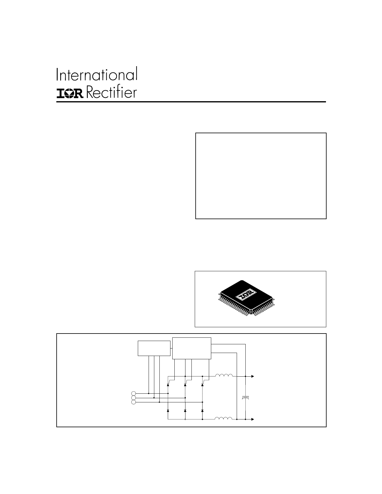
System Block Diagram
Snubber and
Snubber derived
power supply
IR1110
and
Peripheral
Components
AC
3-Phase
Input
(Optional)
+
(Optional)
-
1 page 
ADVANCE INFORMATION
IR1110
DC Electrical Characteristics
RBIAS = 249K/1%, VDD = 5.1V, VSS = 5.1V and TA = 25°C unless otherwise specified.
Symbol
Definition
VDD
VSS
IDD
ISS
VIN
VBREF
VIL1
VIH1
VPCINT
Positive Supply Voltage
Negative Supply Voltage
VDD Supply Current
VSS Supply Current
Input Voltage Range for UIN, VIN, and WIN
Input Voltage Range for VBREF
Input logic low voltage on 1PHEN, LNLSSL
Input logic high voltage on 1PHEN, LNLSSL
Positive Output Voltage Swing at CINTU, CINTV,
and CINTW Pins
VPCR+
VPCR-
I1PHCAP+
I1PHCAP-
I3PHCAP+
I3PHCAP-
VOLLED
Positive Output Voltage Swing at CRAMP Pin
Negative Output Voltage Swing at CRAMP Pin
Sourcing Current at 1PHCAP pin
Sinking Current at 1PHCAP pin
Sourcing Current at 3PHCAP pin
Sinking Current at 3PHCAP pin
Output Low Voltage at 1PHLED, LNLSLED, and
LNLED pins
VOHLED Output High Voltage at 1PHLED, LNLSLED,
and LNLSLED pin
UVLO Undervoltage lockout between VDD-GND
IUVLO+ Sinking Current at UVLOCAP pin
VHSCR Output Voltage at High level at SCRU, SCRV,
and SCRW pins
VLSCR
Output Voltage at Low level at SCRU, SCRV,
and SCRW pins
VRAMPBUF Output Voltage at VRAMP pin
RVBREF Input Resistance On VBREF pin
IBDIPCAP
VtLNLED+
VtLNLED-
VtLNLS
Vt1PH
Sourcing Current of BDIPCAP pin
Peak threshold voltage on UIN/VIN/WIN pins
for LNLED to switch low
Peak threshold voltage on UIN/VIN/WIN pins
for LNLED to switch high
Peak threshold voltage on UIN/VIN/WIN pins
for LNLSLED to stay low
Peak threshold voltage on UIN/VIN/WIN pins
for 1PHLED to stay low
See notes on page 6
www.irf.com
Min.
4.8
-4.8
—-
—-
1.5
0
—-
2.2
—-
—-
0
—-
—-
—-
—-
0
VDD
0.4
4.1
60
—-
Typ. Max. Units Test Conditions
5.1 5.6
-5.1 -5.6
V
Note 3
Note 3
3.0 6.0
-3.0 -5.0
mA
Note 4
Note 4
—- 4.0
—- 5.0
Note 1
—- -2.0
—- —-
V
4.0 4.5
Peak voltage of Vin
= 4.0V
4.0 4.5
—- —-
2.0 —-
1PHCAP=VSS
5.0 —- µA 1PHCAP=GND
3.0 —-
3PHCAP=VSS
15.0 —-
3PHCAP=GND
0.12 .4
Output sinking
—- VDD
V
current = 3.0mA
Output sourcing
current = 3mA
4.4 4.6
86 110 uA VUVLOCAP=VDD
4.5 —-
IO = 1mA
—- 0.1 0.31 V
IO = -1mA
—- 4.0 —-
—- 400 —-
—- 5 —-
2.2 2.3 2.4
kΩ
uA
BDIPCAP=VSS
VLNSET = 1.0V
2.0 2.1 2.2
Note 2
—- .5 —-
All input voltages
V present
—- .5 —-
All input voltages
present
5
5 Page 
ADVANCE INFORMATION
IR1110
Typical Connection Diagram
To
SCRs
CU RU
RGU
RDU
QU
+15V
CV RV CW
RGV
RDV
QV
RGW
VDD
RSG2
RSG1
VDD
CINTW
RINTW
RINTRW
CINTV
RINTV
RINTRV
CINTW
RINTW
RINTRW
52 AVDD
53 CINTW
54 INTNW
55 RINTW
56 RSTRW
57 CINTV
58 INTNV
59 RINTV
60 RSTRV
61 CINTU
62 INTNU
63 RINTU
64 RSTRU
RW
OPTO1
RDW
VDD
OPTO2
QW
RLED2
RLED1
IR1110
MQFP64
Non Square
CWDV
CWDU
RLS2
CPK
C W D WR P K F I L
RPKD
RLS1
RWDU
RWDV
RWDW
VDD
32 VINTDISC2
31 DVSS
BDIPHLD 30
BDIP1 29
BDIPCAP 28
BDIP2 27
RDFIL
RDIP1
CBDIP1
CHOLD
RDIP2
AGND 26
AGND 25
UVLOCAP 24
VPKLL 23
RBIAS 22
RRAMP 21
CRAMP
20
CBDIP2
CUVLO
RPKLL1
RB
RRAMP
CRAMP
CPKLL
DRAMP
U
V
W
DC-
DC+
RU1
RV1
RW1
RNEG1
RPOS1
RU2
RW2
RV2
VDD
R P O S 2 VBUS
REF
RNEG2
RCLAMP1
RERR C1PH
VSS
CERR
C3PH
RCLAMP2
RPKLL2
VDD
Figure 3
www.irf.com
11
11 Page | ||
| Páginas | Total 30 Páginas | |
| PDF Descargar | [ Datasheet IR1110.PDF ] | |
Hoja de datos destacado
| Número de pieza | Descripción | Fabricantes |
| IR1110 | SOFT START CONTROLLER IC | International Rectifier |
| Número de pieza | Descripción | Fabricantes |
| SLA6805M | High Voltage 3 phase Motor Driver IC. |
Sanken |
| SDC1742 | 12- and 14-Bit Hybrid Synchro / Resolver-to-Digital Converters. |
Analog Devices |
|
DataSheet.es es una pagina web que funciona como un repositorio de manuales o hoja de datos de muchos de los productos más populares, |
| DataSheet.es | 2020 | Privacy Policy | Contacto | Buscar |