|
|
PDF UPD4482323 Data sheet ( Hoja de datos )
| Número de pieza | UPD4482323 | |
| Descripción | (UPD4482163/2183/2323/2363) 8M-BIT CMOS SYNCHRONOUS FAST SRAM PIPELINED OPERATION DOUBLE CYCLE DESELECT | |
| Fabricantes | NEC | |
| Logotipo |  |
|
Hay una vista previa y un enlace de descarga de UPD4482323 (archivo pdf) en la parte inferior de esta página. Total 28 Páginas | ||
|
No Preview Available !
DATA SHEET
MOS INTEGRATED CIRCUIT
µPD4482163, 4482183, 4482323, 4482363
8M-BIT CMOS SYNCHRONOUS FAST SRAM
PIPELINED OPERATION
DOUBLE CYCLE DESELECT
Description
The µPD4482163 is a 524,288-word by 16-bit, the µPD4482183 is a 524,288-word by 18-bit, µPD4482323 is a 262,144-
word by 32-bit and the µPD4482363 is a 262,144-word by 36-bit synchronous static RAM fabricated with advanced CMOS
technology using Full-CMOS six-transistor memory cell.
The µPD4482163, µPD4482183, µPD4482323 and µPD4482363 integrates unique synchronous peripheral circuitry, 2-
bit burst counter and output buffer as well as SRAM core. All input registers are controlled by a positive edge of the single
clock input (CLK).
The µPD4482163, µPD4482183, µPD4482323 and µPD4482363 are suitable for applications which require synchronous
operation, high speed, low voltage, high density and wide bit configuration, such as cache and buffer memory.
ZZ has to be set LOW at the normal operation. When ZZ is set HIGH, the SRAM enters Power Down State (“Sleep”). In
the “Sleep” state, the SRAM internal state is preserved. When ZZ is set LOW again, the SRAM resumes normal operation.
The µPD4482163, µPD4482183, µPD4482323 and µPD4482363 are packaged in 100-pin PLASTIC LQFP with a 1.4
mm package thickness for high density and low capacitive loading.
Features
• Single 3.3 V power supply
• Synchronous operation
• Operating temperature : TA = 0 to 70 °C (-A44, -A50, -A60)
TA = −40 to +85 °C (-A44Y, -A50Y, -A60Y)
• Internally self-timed write control
• Burst read / write : Interleaved burst and linear burst sequence
• Fully registered inputs and outputs for pipelined operation
• Double-Cycle deselect timing
• All registers triggered off positive clock edge
• 3.3 V LVTTL Compatible : All inputs and outputs
• Fast clock access time : 2.8 ns (225 MHz), 3.1 ns (200 MHz), 3.5 ns (167 MHz)
• Asynchronous output enable : /G
• Burst sequence selectable : MODE
• Sleep mode : ZZ (ZZ = Open or Low : Normal operation)
• Separate byte write enable : /BW1 to /BW4, /BWE (µPD4482323, µPD4482363)
/BW1, /BW2, /BWE (µPD4482163, µPD4482183)
Global write enable : /GW
• Three chip enables for easy depth expansion
• Common I/O using three state outputs
The information in this document is subject to change without notice. Before using this document, please
confirm that this is the latest version.
Not all products and/or types are available in every country. Please check with an NEC Electronics
sales representative for availability and additional information.
Document No. M14904EJ3V0DS00 (3rd edition)
Date Published December 2002 NS CP(K)
Printed in Japan
TheTmhearmkarks#hoswhoswmsamjoar jroervriesveidsepdoipnotsin. ts.
2000
1 page 
µPD4482163, 4482183, 4482323, 4482363
100-pin PLASTIC LQFP (14 x 20)
[µPD4482323GF, µPD4482363GF]
Marking Side
I/OP3, NC
I/O17
I/O18
VDDQ
VSSQ
I/O19
I/O20
I/O21
I/O22
VSSQ
VDDQ
I/O23
I/O24
NC
VDD
NC
VSS
I/O25
I/O26
VDDQ
VSSQ
I/O27
I/O28
I/O29
I/O30
VSSQ
VDDQ
I/O31
I/O32
I/OP4, NC
100 99 98 97 96 95 94 93 92 91 90 89 88 87 86 85 84 83 82 81
1 80
2 79
3 78
4 77
5 76
6 75
7 74
8 73
9 72
10 71
11 70
12 69
13 68
14 67
15 66
16 65
17 64
18 63
19 62
20 61
21 60
22 59
23 58
24 57
25 56
26 55
27 54
28 53
29 52
30 51
31 32 33 34 35 36 37 38 39 40 41 42 43 44 45 46 47 48 49 50
I/OP2, NC
I/O16
I/O15
VDDQ
VSSQ
I/O14
I/O13
I/O12
I/O11
VSSQ
VDDQ
I/O10
I/O9
VSS
NC
VDD
ZZ
I/O8
I/O7
VDDQ
VSSQ
I/O6
I/O5
I/O4
I/O3
VSSQ
VDDQ
I/O2
I/O1
I/OP1, NC
Remark Refer to Package Drawing for the 1-pin index mark.
Data Sheet M14904EJ3V0DS
5
5 Page 
µPD4482163, 4482183, 4482323, 4482363
Electrical Specifications
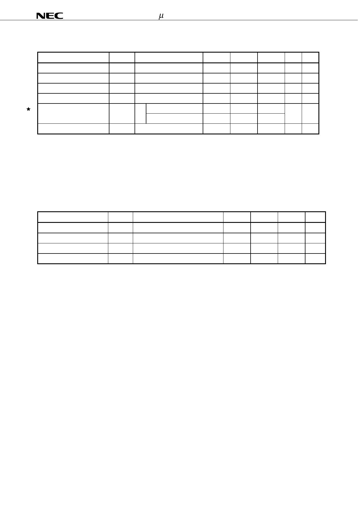
Absolute Maximum Ratings
Parameter
Symbol
Conditions
Supply voltage
Output supply voltage
VDD
VDDQ
Input voltage
VIN
Input / Output voltage
Operating ambient temperature
VI/O
TA
-A44, -A50, -A60
-A44Y, -A50Y, -A60Y
Storage temperature
Tstg
Notes 1. –2.0 V (MIN.) (Pulse width : 2 ns)
2. VDDQ + 2.3 V (MAX.) (Pulse width : 2 ns)
MIN.
–0.5
–0.5
–0.5
–0.5
0
–40
–55
TYP.
MAX. Unit Notes
+4.0
V
VDD
V
VDD + 0.5 V
1, 2
VDDQ + 0.5 V 1, 2
70 °C
+85
+125
°C
Caution
Exposing the device to stress above those listed in Absolute Maximum Ratings could cause
permanent damage. The device is not meant to be operated under conditions outside the limits
described in the operational section of this specification. Exposure to Absolute Maximum Rating
conditions for extended periods may affect device reliability.
Recommended DC Operating Conditions
Parameter
Symbol
Supply voltage
VDD
Output supply voltage
VDDQ
High level input voltage
VIH
Low level input voltage
VIL
Note –0.8 V (MIN.) (Pulse Width : 2 ns)
Conditions
MIN.
3.135
3.135
2.0
–0.3 Note
TYP.
3.3
3.3
MAX.
3.465
3.465
VDDQ + 0.3
+0.8
Unit
V
V
V
V
Data Sheet M14904EJ3V0DS
11
11 Page | ||
| Páginas | Total 28 Páginas | |
| PDF Descargar | [ Datasheet UPD4482323.PDF ] | |
Hoja de datos destacado
| Número de pieza | Descripción | Fabricantes |
| UPD4482321 | (UPD4482161/2181/2321/2361) 8M-BIT CMOS SYNCHRONOUS FAST SRAM FLOW THROUGH OPERATION | NEC |
| UPD4482322 | (UPD4482162/2182/2322/2362) 8M-BIT CMOS SYNCHRONOUS FAST SRAM PIPELINED OPERATION SINGLE CYCLE DESELECT | NEC |
| UPD4482323 | (UPD4482163/2183/2323/2363) 8M-BIT CMOS SYNCHRONOUS FAST SRAM PIPELINED OPERATION DOUBLE CYCLE DESELECT | NEC |
| Número de pieza | Descripción | Fabricantes |
| SLA6805M | High Voltage 3 phase Motor Driver IC. |
Sanken |
| SDC1742 | 12- and 14-Bit Hybrid Synchro / Resolver-to-Digital Converters. |
Analog Devices |
|
DataSheet.es es una pagina web que funciona como un repositorio de manuales o hoja de datos de muchos de los productos más populares, |
| DataSheet.es | 2020 | Privacy Policy | Contacto | Buscar |
