|
|
PDF MAX4215 Data sheet ( Hoja de datos )
| Número de pieza | MAX4215 | |
| Descripción | High-Speed / Single-Supply / Gain of @ / Closed-Loop / Rail-to-Rail Buffers with Enable | |
| Fabricantes | Maxim Integrated | |
| Logotipo |  |
|
Hay una vista previa y un enlace de descarga de MAX4215 (archivo pdf) en la parte inferior de esta página. Total 16 Páginas | ||
|
No Preview Available !
19-4754; Rev 0; 12/97
High-Speed, Single-Supply, Gain of +2,
Closed-Loop, Rail-to-Rail Buffers with Enable
_________________General Description
The MAX4214/MAX4215/MAX4217/MAX4219/MAX4222
are precision, closed-loop, gain of +2 (or -1) buffers
featuring high slew rates, high output current drive, and
low differential gain and phase error. They operate with
a single +3.15V to +11V supply or with ±1.575V to ±5.5V
dual supplies. The input common-mode voltage range
extends 100mV beyond the negative power-supply rail,
and the output swings Rail-to-Rail®.
These devices require only 5.5mA of quiescent supply
current while achieving a 230MHz -3dB bandwidth and
a 600V/µs slew rate. In addition, the MAX4215/
MAX4219 have a disable feature that reduces the sup-
ply current to 400µA per buffer. Input voltage noise is
only 10nV/√Hz, and input current noise is only
1.3pA/√Hz. This buffer family is ideal for low-power/low-
voltage applications requiring wide bandwidth, such as
video, communications, and instrumentation systems.
For space-sensitive applications, the MAX4214 comes
in a miniature 5-pin SOT23 package.
_______________Ordering Information
PART
TEMP. RANGE
PIN-
PACKAGE
SOT
TOP MARK
MAX4214EUK-T -40°C to +85°C
MAX4215ESA -40°C to +85°C
MAX4215EUA -40°C to +85°C
MAX4217ESA -40°C to +85°C
MAX4217EUA -40°C to +85°C
MAX4219ESD -40°C to +85°C
MAX4219EEE -40°C to +85°C
MAX4222ESD -40°C to +85°C
MAX4222EEE -40°C to +85°C
5 SOT23-5
8 SO
8 µMAX
8 SO
8 µMAX
14 SO
16 QSOP
14 SO
16 QSOP
ABAH
—
—
—
—
—
—
—
—
____________________________Features
o Internal Precision Resistors for Closed-Loop
Gains of +2V/V or -1V/V
o High Speed:
230MHz -3dB Bandwidth
90MHz 0.1dB Gain Flatness (MAX4219/22)
600V/µs Slew Rate
o Single 3.3V/5.0V Operation
o Outputs Swing Rail-to-Rail
o Input Common-Mode Range Extends Beyond VEE
o Low Differential Gain/Phase Error: 0.03%/0.04°
o Low Distortion at 5MHz:
-72dBc SFDR
-71dB Total Harmonic Distortion
o High Output Drive: ±120mA
o Low 5.5mA Supply Current
o 400µA Shutdown Supply Current (MAX4215/19)
o Space-Saving SOT23-5, µMAX, or QSOP Packages
______________________Selector Guide
PART
MAX4214
MAX4215
MAX4217
MAX4219
MAX4222
NO. OF
AMPS
1
1
2
3
4
ENABLE
No
Yes
No
Yes
No
PIN-PACKAGE
5 SOT23
8 SO/µMAX
8 SO/µMAX
14 SO, 16 QSOP
14 SO, 16 QSOP
________________________Applications
Battery-Powered Instruments
Video Line Driver
Analog-to-Digital Converter Interface
CCD Imaging Systems
Video Routing and Switching Systems
Video Multiplexing Applications
__________________Pin Configurations
TOP VIEW
OUT 1
5 VCC
MAX4214
VEE 2
IN+ 3
4 IN-
Typical Application Circuit appears at end of data sheet.
Rail-to-Rail is a registered trademark of Nippon Motorola, Inc.
SOT23-5
Pin Configurations continued at end of data sheet.
________________________________________________________________ Maxim Integrated Products 1
For free samples & the latest literature: http://www.maxim-ic.com, or phone 1-800-998-8800.
For small orders, phone 408-737-7600 ext. 3468.
1 page 
High-Speed, Single-Supply, Gain of +2,
Closed-Loop, Rail-to-Rail Buffers with Enable
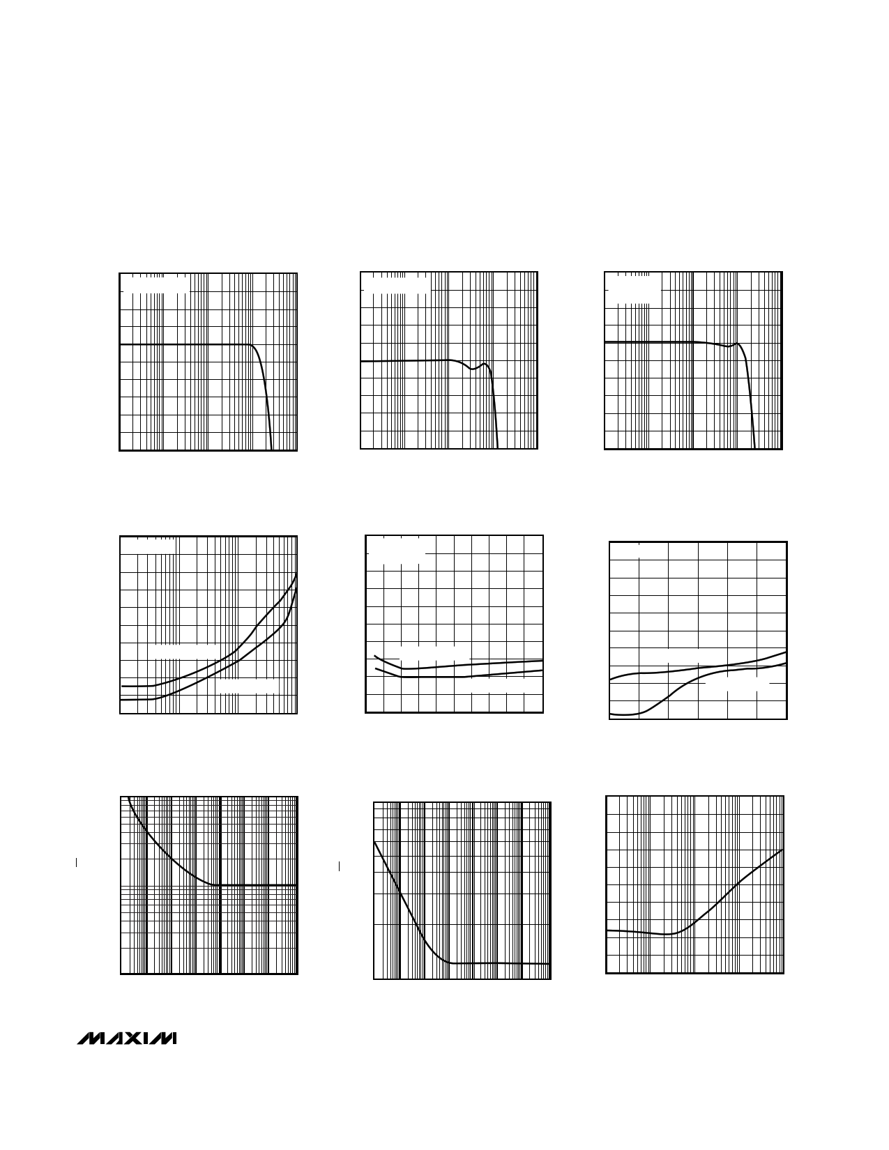
_____________________________Typical Operating Characteristics (continued)
(VCC = +5V, VEE = 0V, AVCL = +2V/V, RL = 100Ω to VCC/2, TA = +25°C, unless otherwise noted.)
MAX4219/MAX4222
SMALL-SIGNAL GAIN vs. FREQUENCY
10
9 VOUT = 100mVp-p
8
7
6
5
4
3
2
1
0
100k
1M 10M 100M
FREQUENCY (Hz)
1G
MAX4219/MAX4222
GAIN FLATNESS vs. FREQUENCY
6.5
6.4 VOUT = 100mVp-p
6.3
6.2
6.1
6.0
5.9
5.8
5.7
5.6
5.5
100k
1M 10M 100M
FREQUENCY (Hz)
1G
MAX4219/MAX4222
LARGE-SIGNAL GAIN vs. FREQUENCY
10
9 VOUT = 2Vp-p
RL = 100Ω
8
7
6
5
4
3
2
1
0
100k
1M 10M 100M
FREQUENCY (Hz)
1G
HARMONIC DISTORTION
vs. FREQUENCY
0
-10 VOUT = 2Vp-p
-20
-30
-40
-50
-60
2ND HARMONIC
-70
-80
3RD HARMONIC
-90
-100
100k
1M 10M
FREQUENCY (Hz)
100M
VOLTAGE-NOISE DENSITY
vs. FREQUENCY
100
10
1
1
10 100 1k 10k 100k 1M 10M
FREQUENCY (Hz)
HARMONIC DISTORTION
vs. RESISTIVE LOAD
0
-10
VOUT = 2Vp-p
f = 5MHz
-20
-30
-40
-50
-60
-70 2ND HARMONIC
-80
3RD HARMONIC
-90
-100
0 100 200 300 400 500 600 700 800 900 1k
RESISTIVE LOAD (Ω)
CURRENT-NOISE DENSITY
vs. FREQUENCY
10
1
1
10 100 1k 10k 100k 1M 10M
FREQUENCY (Hz)
HARMONIC DISTORTION
vs. VOLTAGE SWING
0
f = 5MHz
-10
-20
-30
-40
-50
-60
2ND HARMONIC
-70
-80 3RD HARMONIC
-90
-100
0.5
1.0 1.5 2.0 2.5 3.0
VOLTAGE SWING (Vp-p)
3.5
MAX4217/MAX4219/MAX4222
CROSSTALK vs. FREQUENCY
50
30
10
-10
-30
-50
-70
-90
-110
-130
-150
100k
1M 10M 100M
FREQUENCY (Hz)
1G
_______________________________________________________________________________________ 5
5 Page 
High-Speed, Single-Supply, Gain of +2,
Closed-Loop, Rail-to-Rail Buffers with Enable
MAX4214
MAX4215
MAX4217
MAX4219
IN+ MAX4222
OUT
IN-
500Ω
500Ω
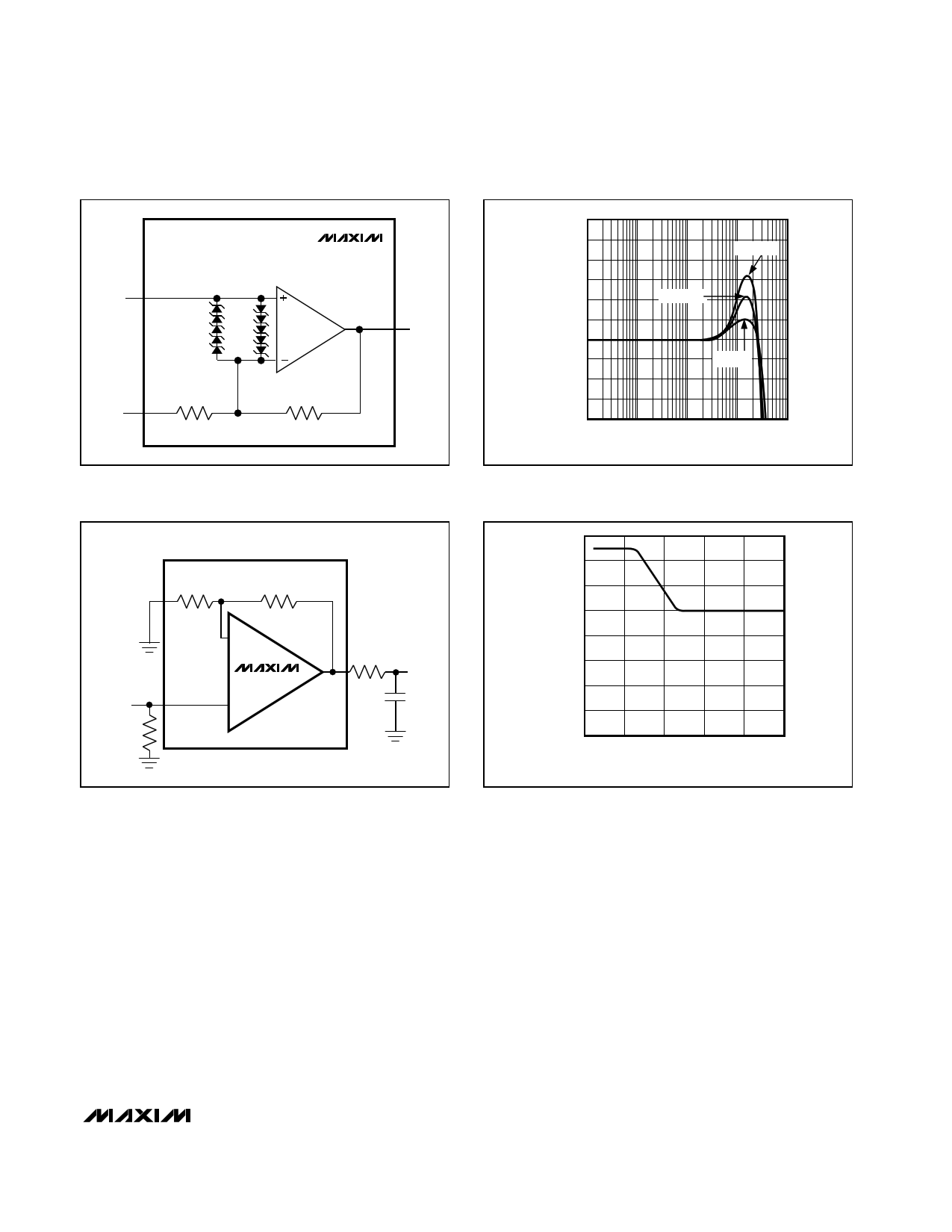
Figure 5. Input Protection Circuit
6
5
4
3
2
1
0
-1
-2
-3
-4
100k
CL = 15pF
CL = 10pF
CL = 5pF
1M 10M 100M
FREQUENCY (Hz)
1G
Figure 6. Small-Signal Gain vs. Frequency with Load
Capacitance and No Isolation Resistor
500Ω
500Ω
VIN
RTIN
50Ω
MAX42_ _
RISO
VOUT
CL
16
14
12
10
8
6
4
2
0
0
50 100 150 200 250
CLOAD (pF)
Figure 7. Driving a Capacitive Load Through an Isolation
Resistor
Figure 8. Isolation Resistance vs. Capacitive Load
Driving large capacitive loads increases the chance of
oscillations occurring in most amplifier circuits. This is
especially true for circuits with high loop gains, such as
voltage followers. The buffer’s output resistance and the
load capacitor combine to add a pole and excess phase
to the loop response. If the frequency of this pole is low
enough to interfere with the loop response and degrade
phase margin sufficiently, oscillations can occur.
A second problem when driving capacitive loads
results from the amplifier’s output impedance, which
looks inductive at high frequencies. This inductance
forms an L-C resonant circuit with the capacitive load,
which causes peaking in the frequency response and
degrades the amplifier’s gain margin.
Figure 6 shows the devices’ frequency response under
different capacitive loads. To drive loads with greater
than 20pF of capacitance or to settle out some of the
peaking, the output requires an isolation resistor like
the one shown in Figure 7. Figure 8 is a graph of the
optimal isolation resistor versus load capacitance.
Figure 9 shows the frequency response of the
MAX4214/MAX4215/MAX4217/MAX4219/MAX4222
when driving capacitive loads with a 27Ω isolation
resistor.
Coaxial cables and other transmission lines are easily
driven when properly terminated at both ends with their
characteristic impedance. Driving back-terminated
transmission lines essentially eliminates the lines’
capacitance.
______________________________________________________________________________________ 11
11 Page | ||
| Páginas | Total 16 Páginas | |
| PDF Descargar | [ Datasheet MAX4215.PDF ] | |
Hoja de datos destacado
| Número de pieza | Descripción | Fabricantes |
| MAX4210 | High-Side Power and Current Monitors | Maxim Integrated |
| MAX4211 | High-Side Power and Current Monitors | Maxim Integrated |
| MAX4212 | Miniature / 300MHz / Single-Supply / Rail-to-Rail Op Amps with Enable | Maxim Integrated |
| MAX4213 | (MAX4212 - MAX4220) Miniature / 300MHz / Single-Supply / Rail-to-Rail Op Amps | Maxim Integrated |
| Número de pieza | Descripción | Fabricantes |
| SLA6805M | High Voltage 3 phase Motor Driver IC. |
Sanken |
| SDC1742 | 12- and 14-Bit Hybrid Synchro / Resolver-to-Digital Converters. |
Analog Devices |
|
DataSheet.es es una pagina web que funciona como un repositorio de manuales o hoja de datos de muchos de los productos más populares, |
| DataSheet.es | 2020 | Privacy Policy | Contacto | Buscar |
