|
|
|
PDF NCP302 Data sheet ( Hoja de datos )
| Número de pieza | NCP302 | |
| Descripción | Voltage Detector Series with Programmable Delay | |
| Fabricantes | ON | |
| Logotipo | ||
1. NCP302 Hay una vista previa y un enlace de descarga de NCP302 (archivo pdf) en la parte inferior de esta página. Total 25 Páginas | ||
|
No Preview Available !
NCP302, NCP303
Voltage Detector Series
with Programmable Delay
The NCP302 and NCP303 series are second generation ultra−low
current voltage detectors that contain a programmable time delay
generator. These devices are specifically designed for use as reset
controllers in portable microprocessor based systems where extended
battery life is paramount.
Each series features a highly accurate undervoltage detector with
hysteresis and an externally programmable time delay generator. This
combination of features prevents erratic system reset operation.
The NCP302 series consists of complementary output devices that
are available with either an active high or active low reset. The
NCP303 series has an open drain N−Channel output with an active low
reset output.
Features
• Quiescent Current of 0.5 mA Typical
• High Accuracy Undervoltage Threshold of 2.0%
• Externally Programmable Time Delay Generator
• Wide Operating Voltage Range of 0.8 V to 10 V
• Complementary or Open Drain Output
• Active Low or Active High Reset
• Pb−Free Packages are Available
Typical Applications
• Microprocessor Reset Controller
• Low Battery Detection
• Power Fail Indicator
• Battery Backup Detection
http://onsemi.com
5
1
THIN SOT23−5/TSOP−5/SC59−5
CASE 483
PIN CONNECTIONS AND
MARKING DIAGRAM
Reset 1
Output
Input 2
5 CD
Ground 3
4 N.C.
(Top View)
xxx =Specific Device Code
Y = Year
W = Work Week
ORDERING INFORMATION
See detailed ordering and shipping information in the ordering
information section on page 22 of this data sheet.
NCP302xSNxxT1
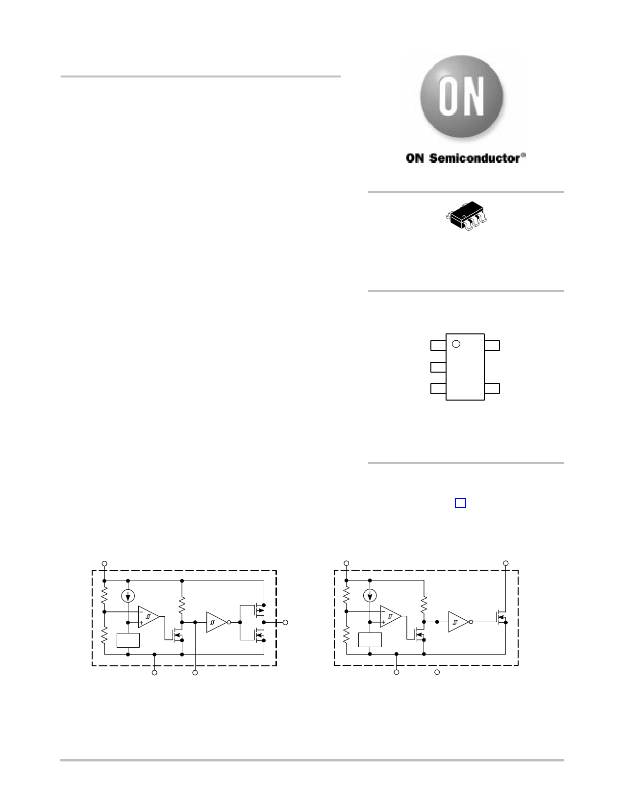
Complementary Output Configuration
2 Input
NCP303LSNxxT1
Open Drain Output Configuration
2 Input
1 Reset Output
RD
1
RD
* Reset
Vref
Output
Vref
3 GND 5 CD
3 GND 5 CD
* Inverter for active low devices.
* Buffer for active high devices.
This device contains 28 active transistors.
Figure 1. Representative Block Diagrams
© Semiconductor Components Industries, LLC, 2004
October, 2004 − Rev. 14
1
Publication Order Number:
NCP302/D
1 page 
NCP302, NCP303
ELECTRICAL CHARACTERISTICS (continued) (For all values TA = 25°C, unless otherwise noted.)
Characteristic
Symbol Min Typ Max Unit
NCP302/3− 2.7
ÁÁÁÁÁÁÁÁÁÁÁÁÁÁÁÁÁÁÁÁÁÁÁÁÁÁÁÁÁÁÁÁÁÁÁÁÁÁÁÁÁÁÁÁÁÁÁÁÁÁÁÁÁÁÁÁÁÁÁÁÁÁÁÁÁÁReset Output Current (Pin 1, Active High ‘H’ Suffix Devices)
IOUT
mA
Nch Sink Current, NCP302, NCP303
(VOUT = 0.5 V, Vin = 5.0 V)
6.3 11
−
Pch Source Current, NCP302
(VOUT = 0.4 V, Vin = 0.7 V)
(VOUT = GND, Vin = 1.5 V)
0.011
0.525
0.04
0.6
−
−
CD Delay Pin Threshold Voltage (Pin 5)
VTCD
V
(Vin = 2.97 V)
ÁÁÁÁÁÁÁÁÁÁÁÁÁÁÁÁÁÁÁÁÁÁÁÁÁÁÁÁÁÁÁÁÁDelay Capacitor Pin Sink Current (Pin 5)
(Vin = 0.7 V, VCD = 0.1V)
ÁÁÁÁÁÁÁÁÁÁÁÁÁÁÁÁÁÁÁÁÁÁÁÁÁÁÁÁÁÁÁÁÁÁÁÁÁÁÁÁÁÁÁÁÁÁÁÁÁÁÁÁÁÁÁÁÁÁÁÁÁÁÁÁÁÁ(Vin = 1.5 V, VCD = 0.5V)
1.49 2.01 2.53
ICD mA
2.0 120
−
200 1600
−
Delay Pullup Resistance (Pin 5)
RD 0.5 1.0 2.0 MW
NCP302/3 − 3.0
ÁÁÁÁÁÁÁÁÁÁÁÁÁÁÁÁÁÁÁÁÁÁÁÁÁÁÁÁÁÁÁÁÁDetector Threshold (Pin 2, Vin Decreasing)
ÁÁÁÁÁÁÁÁÁÁÁÁÁÁÁÁÁÁÁÁÁÁÁÁÁÁÁÁÁÁÁÁÁDetector Threshold Hysteresis (Pin 2, Vin Increasing)
ÁÁÁÁÁÁÁÁÁÁÁÁÁÁÁÁÁÁÁÁÁÁÁÁÁÁÁÁÁÁÁÁÁSupply Current (Pin 2)
ÁÁÁÁÁÁÁÁÁÁÁÁÁÁÁÁÁÁÁÁÁÁÁÁÁÁÁÁÁÁÁÁÁ(Vin = 2.87 V)
ÁÁÁÁÁÁÁÁÁÁÁÁÁÁÁÁÁÁÁÁÁÁÁÁÁÁÁÁÁÁÁÁÁ(Vin = 5.0 V)
VDET−
VHYS
Iin
2.94 3.00 3.06
V
0.09 0.15 0.21
V
mA
− 0.27 0.9
− 0.47 1.3
Maximum Operating Voltage (Pin 2)
Vin(max)
−
− 10 V
Minimum Operating Voltage (Pin 2)
(TA = −40°C to 85°C)
ÁÁÁÁÁÁÁÁÁÁÁÁÁÁÁÁÁÁÁÁÁÁÁÁÁÁÁÁÁÁÁÁÁÁÁÁÁÁÁÁÁÁÁÁÁÁÁÁÁÁÁÁÁÁÁÁÁÁÁÁÁÁÁÁÁÁReset Output Current (Pin 1, Active Low ‘L’ Suffix Devices)
Vin(min)
IOUT
−
0.55 0.70
V
− 0.65 0.80
mA
Nch Sink Current, NCP302, NCP303
(VOUT = 0.05V, Vin = 0.70V)
0.01 0.05
−
(VOUT = 0.50V, Vin = 1.5V)
1.0 2.0
−
Pch Source Current, NCP302
(VOUT = 2.4V, Vin = 4.5V)
ÁÁÁÁÁÁÁÁÁÁÁÁÁÁÁÁÁÁÁÁÁÁÁÁÁÁÁÁÁÁÁÁÁÁÁÁÁÁÁÁÁÁÁÁÁÁÁÁÁÁÁÁÁÁÁÁÁÁÁÁÁÁÁÁÁÁReset Output Current (Pin 1, Active High ‘H’ Suffix Devices)
IOUT
1.0 6.0
−
mA
Nch Sink Current, NCP302, NCP303
(VOUT = 0.5 V, Vin = 5.0 V)
6.3 11
−
Pch Source Current, NCP302
(VOUT = 0.4 V, Vin = 0.7 V)
(VOUT = GND, Vin = 1.5 V)
0.011
0.525
0.04
0.6
−
−
CD Delay Pin Threshold Voltage (Pin 5)
VTCD
V
(Vin = 3.3 V)
ÁÁÁÁÁÁÁÁÁÁÁÁÁÁÁÁÁÁÁÁÁÁÁÁÁÁÁÁÁÁÁÁÁDelay Capacitor Pin Sink Current (Pin 5)
(Vin = 0.7 V, VCD = 0.1V)
ÁÁÁÁÁÁÁÁÁÁÁÁÁÁÁÁÁÁÁÁÁÁÁÁÁÁÁÁÁÁÁÁÁ(Vin = 1.5 V, VCD = 0.5V)
ÁÁÁÁÁÁÁÁÁÁÁÁÁÁÁÁÁÁÁÁÁÁÁÁÁÁÁÁÁÁÁÁÁDelay Pullup Resistance (Pin 5)
1.65 2.23 2.81
ICD mA
2.0 120
−
200 1600
−
RD 0.5 1.0 2.0 MW
NCP302/3 − 4.5
ÁÁÁÁÁÁÁÁÁÁÁÁÁÁÁÁÁÁÁÁÁÁÁÁÁÁÁÁÁÁÁÁÁDetector Threshold (Pin 2, Vin Decreasing)
ÁÁÁÁÁÁÁÁÁÁÁÁÁÁÁÁÁÁÁÁÁÁÁÁÁÁÁÁÁÁÁÁÁDetector Threshold Hysteresis (Pin 2, Vin Increasing)
ÁÁÁÁÁÁÁÁÁÁÁÁÁÁÁÁÁÁÁÁÁÁÁÁÁÁÁÁÁÁÁÁÁSupply Current (Pin 2)
ÁÁÁÁÁÁÁÁÁÁÁÁÁÁÁÁÁÁÁÁÁÁÁÁÁÁÁÁÁÁÁÁÁ(Vin = 4.34 V)
ÁÁÁÁÁÁÁÁÁÁÁÁÁÁÁÁÁÁÁÁÁÁÁÁÁÁÁÁÁÁÁÁÁ(Vin = 6.5 V)
VDET−
VHYS
Iin
4.410
0.135
−
−
4.500
0.225
0.33
0.52
4.590
0.315
1.0
1.4
V
V
mA
Maximum Operating Voltage (Pin 2)
Vin(max)
−
− 10 V
Minimum Operating Voltage (Pin 2)
(TA = −40°C to 85°C)
Vin(min)
−
0.55 0.70
V
− 0.65 0.80
http://onsemi.com
5
5 Page 
NCP302, NCP303
0.98
0.96
0.94
VDET+
0.92
0.90
VDET−
0.88
0.86
−50 −25 0 25 50 75 100
TA, AMBIENT TEMPERATURE (°C)
Figure 3. NCP302/3 Series 0.9 V
Detector Threshold Voltage vs. Temperature
3.00
2.95
2.90
2.85
VDET+
2.80
2.75
2.70
VDET−
2.65
2.60
−50 −25 0 25 50 75 100
TA, AMBIENT TEMPERATURE (°C)
Figure 4. NCP302/3 Series 2.7 V
Detector Threshold Voltage vs. Temperature
4.9
4.8
VDET+
4.7
4.6
VDET−
4.5
4.4
4.3
−50 −25 0 25 50 75 100
TA, AMBIENT TEMPERATURE (°C)
Figure 5. NCP302/3 Series 4.5 V
Detector Threshold Voltage vs. Temperature
0.9
Vin = 0.99 V
0.8
0.7
0.6
0.5
0.4
0.3
−50 −25 0 25 50 75 100
TA, AMBIENT TEMPERATURE (°C)
Figure 6. NCP302/3 Series 0.9 V
CD Delay Pin Threshold Voltage vs. Temperature
2.3
Vin = 2.97 V
2.2
2.1
2.0
1.9
1.8
−50 −25 0 25 50 75 100
TA, AMBIENT TEMPERATURE (°C)
Figure 7. NCP302/3 Series 2.7 V
CD Delay Pin Threshold Voltage vs. Temperature
3.3
Vin = 4.95 V
3.2
3.1
3.0
2.9
2.8
2.7
−50 −25 0 25 50 75 100
TA, AMBIENT TEMPERATURE (°C)
Figure 8. NCP302/3 Series 4.5 V
CD Delay Pin Threshold Voltage vs. Temperature
http://onsemi.com
11
11 Page | ||
| Páginas | Total 25 Páginas | |
| PDF Descargar | [ Datasheet NCP302.PDF ] | |
Hoja de datos destacado
| Número de pieza | Descripción | Fabricantes |
| NCP300 | Voltage Detector Series | ON |
| NCP300HSN09T1 | Voltage Detector Series | ON |
| NCP300HSN10T1 | Voltage Detector Series | ON |
| NCP300HSN11T1 | Voltage Detector Series | ON |
| Número de pieza | Descripción | Fabricantes |
| SLA6805M | High Voltage 3 phase Motor Driver IC. |
Sanken |
| SDC1742 | 12- and 14-Bit Hybrid Synchro / Resolver-to-Digital Converters. |
Analog Devices |
|
DataSheet.es es una pagina web que funciona como un repositorio de manuales o hoja de datos de muchos de los productos más populares, |
| DataSheet.es | 2020 | Privacy Policy | Contacto | Buscar |