|
|
|
PDF PI6C2408-1LE Data sheet ( Hoja de datos )
| Número de pieza | PI6C2408-1LE | |
| Descripción | Zero-Delay Clock Buffer | |
| Fabricantes | Pericom Semiconductor Corporation | |
| Logotipo | ||
Hay una vista previa y un enlace de descarga de PI6C2408-1LE (archivo pdf) en la parte inferior de esta página. Total 10 Páginas | ||
|
No Preview Available !
PI6C24081122334455667788990011223344556677889900112233445566778899001122112233445566778899001122334455667788990011223344556677889900112211223344556677889900112233445566778899001122334455667788990011221122334455667788990011223344556677889900112233445566778899001122112233445566778899001122
Zero-Delay Clock Buffer
Features
• Maximum rated frequency: 140 MHz
• Low cycle-to-cycle jitter
• Input to output delay, less than 150ps
• External feedback pin allows outputs to be synchronized
to the clock input
• 5V tolerant input*
• Operates at 3.3V VDD
• Test mode allows bypass of the PLL for system testing
purposes (e.g., IBIS measurements)
• Clock frequency multipliers ½x to 4x dependent on option
• Packaging (Pb-free and Green available):
-16-pin, 150-mil SOIC (W)
-16-pin173-milTSSOP (L)
* FB_IN and CLKIN must reference the same voltage thresh-
olds for the PLL to deliver zero delay skewing
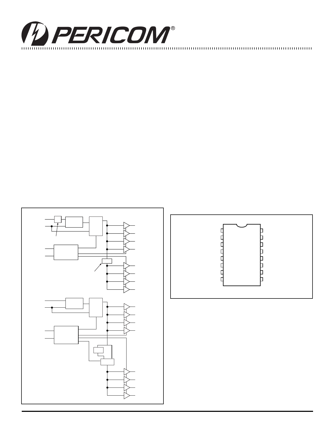
Block Diagram
FB_IN
CLKIN
÷2 PLL
Option (-3, -4)
SEL1
SEL2
Decode
Logic
MUX
÷2
Option (-2, -3)
PI6C2408 (-1, -1H, -2, -3, -4)
FB_IN
CLKIN
PLL
MUX
SEL2
SEL1
Decode
Logic
PI6C2408-6
÷2
MUX
OUTA1
OUTA2
OUTA3
OUTA4
OUTB1
OUTB2
OUTB3
OUTB4
OUTA1
OUTA2
OUTA3
OUTA4
OUTB1
OUTB2
OUTB3
OUTB4
Description
The PI6C2408 is a PLL-based, zero-delay buffer, with the ability
to distribute eight outputs of up to 140 MHz at 3.3 V. Two banks of
four outputs exist, and, depending on product option ordered, can
supply either reference frequency, prescaled half frequency, or
multiplied2xor4xinputclockfrequencies. ThePI6C2408familyhas
a power-sparing feature: when input SEL2 is 0, the component will
3-state one or both banks of outputs depending on the state of input
SEL1. A PLL bypass test mode also exists. This product line is
available in high-drive and industrial environment versions.
An external feedback pin is used to synchronize the outputs to the
input; the relationship between loading of this signal and the other
outputs determines the input-output delay.
The PI6C2408 is characterized for both commercial and industrial
operation.
Pin Configuration
CLKIN
OUTA1
OUTA2
VDD
GND
OUTB1
OUTB2
SEL2
1 16
2 15
3 14
4 16-Pin 13
5 W, L 12
6 11
7 10
89
FB_IN
OUTA4
OUTA3
VDD
GND
OUTB4
OUTB3
SEL1
1 PS8589E 09/15/04
1 page 
PI6C2408
Zero Delay Clock Buffer1122334455667788990011223344556677889900112233445566778899001122112233445566778899001122334455667788990011223344556677889900112211223344556677889900112233445566778899001122334455667788990011221122334455667788990011223344556677889900112233445566778899001122112233445566778899001122
AC Elecrical Characteristics for Industrial Temperature Devices
Parameters
Name
Test Conditions
Min. Typ. Max. Units
FO
tDC
tR
tF
tS K (O )
t0
Output Frequency
30pF load
15pF load
10.0
100
140
MHz
Duty Cycle(1)
(–1, –2, –3, –4, –6)
Measured at VDD/2, FOUT <66.67MHz 30pF load 40.0
Measured at VDD/2, FOUT <140 MHz 15pF load
60.0
Duty Cycle(1) (–1H)
Measured at VDD/2, FOUT <45 MHz 30pF load
45.0
50 55.0 %
Measured at VDD/2, FOUT <66.67MHz 30pF load 45.0
Measured at VDD/2, FOUT <140 MHz 15pF load 40.0
60.0
Measured at VDD/2, FOUT <45MHz 30pF load
45.0
55.0
Rise Time(1) (–1, –2, –3, –4,) Measured between 0.8V and 2.0V, 30pF load
2.2
Measured between 0.8V and 2.0V, 15pF load
1.50
Rise Time(1) (–1H)
Fall Time(1) (–1, –2, –3, –4,)
Measured between 0.8V and 2.0V, 30pF load
Measured between 0.8V and 2.0V, 30pF load
1.50 ns
2.50
Measured between 0.8V and 2.0V, 15pF load
1.50
Fall Time(1) (–1H)
Measured between 0.8V and 2.0V, 30pF load
1.25
Output to Output Skew within
same Bank (–1,–2,–3,–4,–6)(1)
OUTA to OUTB Skew(1)
(–1,–1H,–4)
All outputs equally loaded
200
OUTA to OUTB Skew(1)
(–2,–3,–6)
400 ps
Delay, CLKIN Rising Edge
to FB_IN Rising Edge(1)
Measured at VDD/2
0 ±150
tS K (D)
tSLEW
tJIT
tLO C K
Device-to-Device Skew(1)
Output Slew Rate(1)
Cycle-to-Cycle Jitter(1)
(–1,–1H,–4)
Cycle-to-Cycle Jitter(1)
(–2,–3,–6)
PLL Lock Time(1)
Measured at VDD/2 on FB_IN pins of devices
Measured between 0.8V & 2.0V on –1H device
using Test Crt #2
Measured at 66.67 MHz, loaded 30pF load
Measured at 140 MHz, loaded 15pF load
Measured at 66.67 MHz, loaded 30pF load
Stable power supply, valid clocks
presented on CLKIN and FB_IN pins
0 500
1 V/ns
200
100 ps
400
1.0 ms
Notes:
1. See Switching Waveforms on page 7.
5 PS8589E 09/15/04
5 Page | ||
| Páginas | Total 10 Páginas | |
| PDF Descargar | [ Datasheet PI6C2408-1LE.PDF ] | |
Hoja de datos destacado
| Número de pieza | Descripción | Fabricantes |
| PI6C2408-1L | Zero-Delay Clock Buffer | Pericom Semiconductor Corporation |
| PI6C2408-1LE | Zero-Delay Clock Buffer | Pericom Semiconductor Corporation |
| Número de pieza | Descripción | Fabricantes |
| SLA6805M | High Voltage 3 phase Motor Driver IC. |
Sanken |
| SDC1742 | 12- and 14-Bit Hybrid Synchro / Resolver-to-Digital Converters. |
Analog Devices |
|
DataSheet.es es una pagina web que funciona como un repositorio de manuales o hoja de datos de muchos de los productos más populares, |
| DataSheet.es | 2020 | Privacy Policy | Contacto | Buscar |