|
|
|
PDF MC14013 Data sheet ( Hoja de datos )
| Número de pieza | MC14013 | |
| Descripción | Dual Type D Flip-Flop | |
| Fabricantes | ON Semiconductor | |
| Logotipo | ||
 1. D Flip-Flop ( PDF ) Hay una vista previa y un enlace de descarga de MC14013 (archivo pdf) en la parte inferior de esta página. Total 8 Páginas | ||
|
No Preview Available !
MC14013B
Dual Type D Flip-Flop
The MC14013B dual type D flip–flop is constructed with MOS
P–channel and N–channel enhancement mode devices in a single
monolithic structure. Each flip–flop has independent Data, (D), Direct
Set, (S), Direct Reset, (R), and Clock (C) inputs and complementary
outputs (Q and Q). These devices may be used as shift register
elements or as type T flip–flops for counter and toggle applications.
• Static Operation
• Diode Protection on All Inputs
• Supply Voltage Range = 3.0 Vdc to 18 Vdc
• Logic Edge–Clocked Flip–Flop Design
Logic state is retained indefinitely with clock level either high or low;
information is transferred to the output only on the positive–going
edge of the clock pulse
• Capable of Driving Two Low–power TTL Loads or One Low–power
Schottky TTL Load Over the Rated Temperature Range
• Pin–for–Pin Replacement for CD4013B
MAXIMUM RATINGS (Voltages Referenced to VSS) (Note 2.)
Symbol
Parameter
Value
VDD
Vin, Vout
DC Supply Voltage Range
Input or Output Voltage Range
(DC or Transient)
– 0.5 to +18.0
– 0.5 to VDD + 0.5
Unit
V
V
Iin, Iout
Input or Output Current
(DC or Transient) per Pin
± 10 mA
PD Power Dissipation,
per Package (Note 3.)
500 mW
TA Ambient Temperature Range
Tstg Storage Temperature Range
TL Lead Temperature
(8–Second Soldering)
– 55 to +125
– 65 to +150
260
°C
°C
°C
2. Maximum Ratings are those values beyond which damage to the device
may occur.
3. Temperature Derating:
Plastic “P and D/DW” Packages: – 7.0 mW/_C From 65_C To 125_C
This device contains protection circuitry to guard against damage due to high
static voltages or electric fields. However, precautions must be taken to avoid
applications of any voltage higher than maximum rated voltages to this
v vhigh–impedance circuit. For proper operation, Vin and Vout should be constrained
to the range VSS (Vin or Vout) VDD.
Unused inputs must always be tied to an appropriate logic voltage level (e.g.,
either VSS or VDD). Unused outputs must be left open.
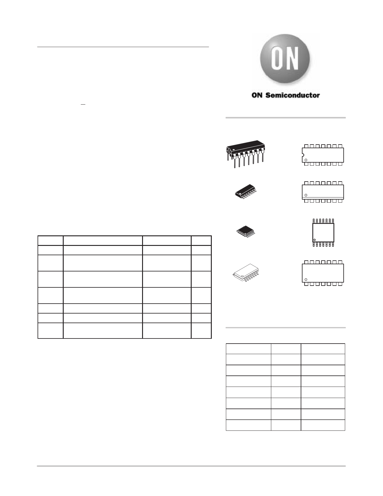
http://onsemi.com
PDIP–14
P SUFFIX
CASE 646
SOIC–14
D SUFFIX
CASE 751A
MARKING
DIAGRAMS
14
MC14013BCP
AWLYYWW
1
14
14013B
AWLYWW
1
TSSOP–14
DT SUFFIX
CASE 948G
14
14
013B
ALYW
SOEIAJ–14
F SUFFIX
CASE 965
1
14
MC14013B
AWLYWW
1
A = Assembly Location
WL or L = Wafer Lot
YY or Y = Year
WW or W = Work Week
ORDERING INFORMATION
Device
Package
Shipping
MC14013BCP
PDIP–14
2000/Box
MC14013BD
SOIC–14
55/Rail
MC14013BDR2 SOIC–14 2500/Tape & Reel
MC14013BDT
TSSOP–14
96/Rail
MC14013BDTR2 TSSOP–14 2500/Tape & Reel
MC14013BF
SOEIAJ–14 See Note 1.
MC14013BFEL SOEIAJ–14 See Note 1.
1. For ordering information on the EIAJ version of
the SOIC packages, please contact your local
ON Semiconductor representative.
© Semiconductor Components Industries, LLC, 2000
March, 2000 – Rev. 3
1
Publication Order Number:
MC14013B/D
1 page 
MC14013B
20 ns
D
tsu (H)
C
90%
50%
10%
tsu (L)
th
tWH
tPLH
Q
1
fcl
90%
50%
10%
tTLH
Inputs R and S low.
20 ns
90%
50%
10%
tWL
VDD
VSS
20 ns
VDD
VSS
tPHL
tTHL
VOH
VOL
Figure 1. Dynamic Signal Waveforms
(Data, Clock, and Output)
20 ns
SET OR
RESET
90%
tw
CLOCK
tPLH
tPHL
Q OR Q
20 ns
50%
10%
20 ns
90%
trem
50%
tw
50%
VDD
VSS
20 ns VDD
10% VSS
VOH
VOL
Figure 2. Dynamic Signal Waveforms
(Set, Reset, Clock, and Output)
D
CLOCK
TYPICAL APPLICATIONS
n–STAGE SHIFT REGISTER
12
DQ
DQ
CQ
CQ
nth
DQ
CQ
Q
CLOCK
BINARY RIPPLE UP–COUNTER (Divide–by–2n)
12
nth
DQ
DQ
DQ
CQ
CQ
CQ
Q
CLOCK
T FLIP–FLOP
MODIFIED RING COUNTER (Divide–by–(n+1))
12
nth
DQ
DQ
DQ
CQ
CQ
CQ
Q
http://onsemi.com
5
5 Page | ||
| Páginas | Total 8 Páginas | |
| PDF Descargar | [ Datasheet MC14013.PDF ] | |
Hoja de datos destacado
| Número de pieza | Descripción | Fabricantes |
| MC14010AL | (MC14009xx / MC14010xx) Buffers | Motorola Semiconductors |
| MC14010CL | (MC14009xx / MC14010xx) Buffers | Motorola Semiconductors |
| MC14010CP | (MC14009xx / MC14010xx) Buffers | Motorola Semiconductors |
| MC14010N | MC14010N / MC14011N | Unitra Cemi |
| Número de pieza | Descripción | Fabricantes |
| SLA6805M | High Voltage 3 phase Motor Driver IC. |
Sanken |
| SDC1742 | 12- and 14-Bit Hybrid Synchro / Resolver-to-Digital Converters. |
Analog Devices |
|
DataSheet.es es una pagina web que funciona como un repositorio de manuales o hoja de datos de muchos de los productos más populares, |
| DataSheet.es | 2020 | Privacy Policy | Contacto | Buscar |