|
|
|
PDF RTC4573 Data sheet ( Hoja de datos )
| Número de pieza | RTC4573 | |
| Descripción | Serial RTC with Alarm and Timer | |
| Fabricantes | Epson Company | |
| Logotipo | ||
Hay una vista previa y un enlace de descarga de RTC4573 (archivo pdf) en la parte inferior de esta página. Total 12 Páginas | ||
|
No Preview Available !
Serial RTC with Alarm and Timer
RTC - 4573
· Built-in frequency adjusted 32.768KHz crystal oscillator
· Serial interface that can be controlled through three signal lines
· Week , Day , hour , and minute alarm interrupt functions
· Interval timer interrupt function that can be set with an interval ranging from 1/4096th of a second to 255minutes
· Dual dedicated interrupt outputs for software maskable alarms and for timers
· Functions that detect halting of crystal oscillation, and when the time is being updated
· Automatic leap year compensation function
· Wide interface voltage range, from 1.6 to 5.5V
· Wide timing voltage range, from 1.6 to 5.5V
· Low current consumption : 0.5mA/3V (typ.)
· Small SOP package suited for high-density mounting
n Overview
This module is a serial interface-type real-time clock with a crystal oscillator on chip. This module includes clock
and calendar circuitry (from seconds to years) with automatic leap year compensation, alarms, and timer interrupt
functions, as well as functions that detect when oscillation is halted, the time is being updated. The serial
interface permits control through three signal lines, keeping the number of ports required on the system side to a
minimum. Because the small SOP package can be used in high-density mounting, this module is ideal for
portable telephones, hand-held terminals, and other compact electronic equipment.
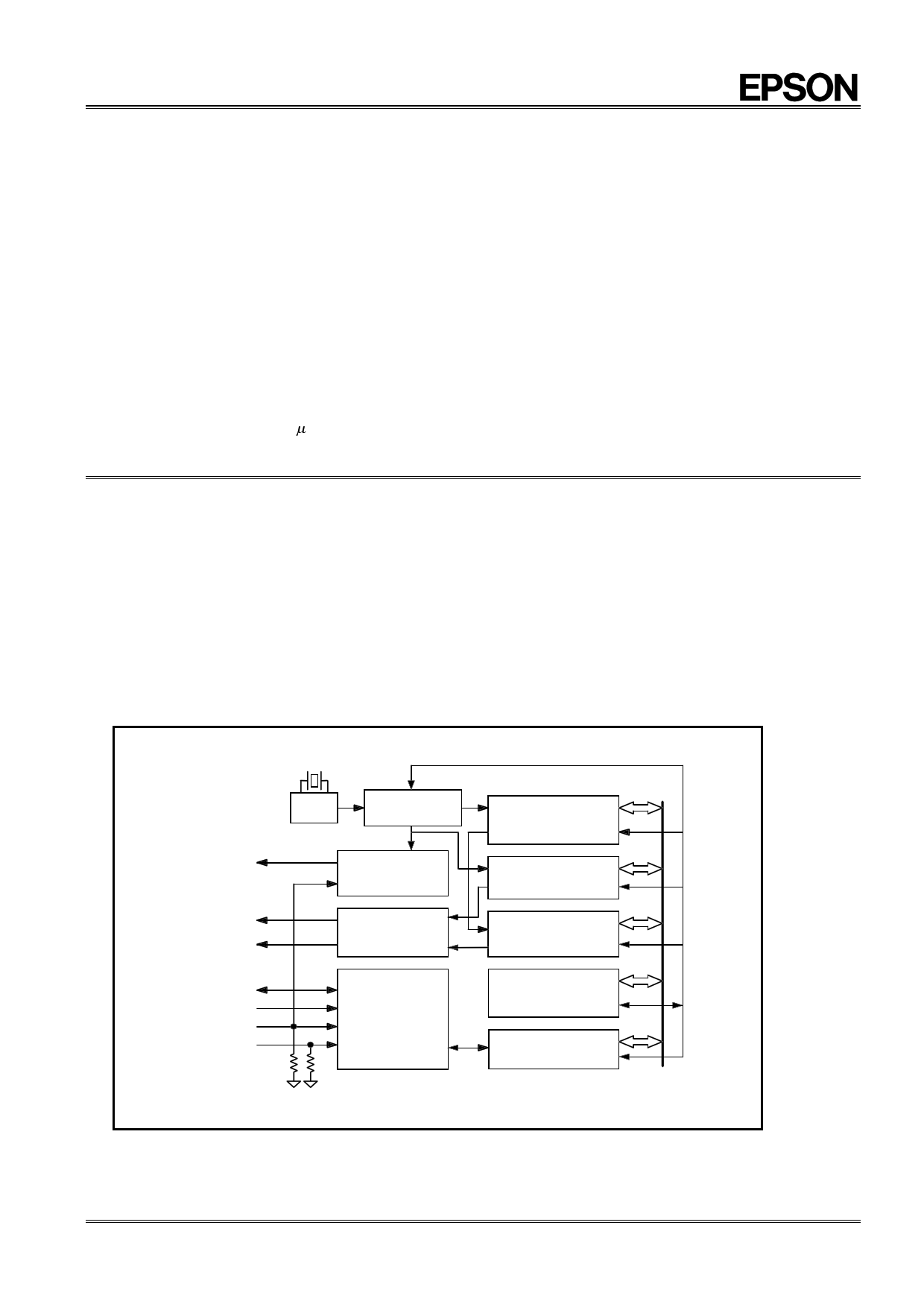
n Block Diagram
FOUT
/ TIRQ
/ AIRQ
DATA
CLK
C E1
C E0
32.768KHz
OSC
DIVIDER
OUTPUT
CONTROLLER
INTERRUPTS
CONTROLLER
BUS
INTERFACE
CIRCUIT
CONTROL LINE
CLOCK and
CALENDAR
TIMER
REGISTER
ALARM
REGISTER
CONTROL
REGISTER
SHIFT REGISTER
Page-1
Aug. 1998
1 page 
n Register Table
Address
0
1
2
3
4
5
6
7
8
9
A
B
C
D
E
F
Function
Sec
Min
Hour
Week
Day
Month
Year
Minutes Alarm
Hours Alarm
Week Alarm
Day Alarm
FOUT control
Timer interrupt control
Count Down Timer
Control 1
Control 2
bit7 bit6 bit5 bit4 bit3 bit2 bit1 bit0
fos 40 20 10
8
4
2
1
fr 40 20 10 8 4 2 1
fr * 20 10 8 4 2 1
fr 6 5 4 3 2 1 0
fr * 20 10 8 4 2 1
fr * * 10 8 4 2 1
80 40 20 10
8
4
2
1
AE 40 20 10
8
4
2
1
AE * 20 10 8 4 2 1
AE 6 5 4 3 2 1 0
AE * 20 10 8 4 2 1
FE * FD4 FD3 * FD2 FD1 FD0
TE * TD1 TD0 * * * *
128 64 32 16
8
4
2
1
* * * TI/TP AF TF AIE TIE
* TEST STOP RESET HOLD * * *
1.1 Timekeeping/calendar registers (register 0 to register 6)
· The data in these registers is BCD format. For example, "0101 1001" represents 59 seconds. In addition, the
"*" mark in the register table means that the register is readable and writable, and can be used as RAM. Time is
kept in the 24-hour format.
· Writing to a bit marked with an asterisk ("*") is permitted; such bits can be used as RAM. When the alarm and
timer functions are not used, registers 7 to A can be used as 8-bit memory registers, and registers C and D can
be used as 7-bit memory registers.
· Year register and leap years
A leap year is detected by dividing the two BCD digits of the year register by four; if the remainder is zero, the
year is a leap year. Therefore, leap years can be automatically determined whether the year is numbered
according to the western calendar or the Japanese calendar (year of Heisei).
· Day of the week
The day of the week register uses 7 bits, from 0 to 6; the meanings of the bits are shown in the table below. Do
not set more than one bit to "1" at any one time.
bit 6
0
0
0
0
0
0
1
bit 5
0
0
0
0
0
1
0
bit 4
0
0
0
0
1
0
0
bit 3
0
0
0
1
0
0
0
bit 2
0
0
1
0
0
0
0
bit 1
0
1
0
0
0
0
0
bit 0
1
0
0
0
0
0
0
day of week
Sunday
Monday
Tuesday
Wednesday
Thursday
Friday
Saturday
· fos ( OSC Flag )
This flag uses it for a monitor of battery listing degradation with the binary digit which that oscillation stopped is
set at. Oscillation stopping shows "1", and it is cleared by writing in "0". But fo flag can't write in "0" when
oscillation stopped. And fo can write in "1", but don't write in it. Other binary digit (HOLD,STOP,RESET) doesn't
receive affect even in case of "1".
· fr ( READ Flag )
It is the binary digit that turn into "1" when CE was input, and carry occurred during "H" for 1 second. The distinction
that carry to a figure rose during (CE input ="H" during readout of register in an indicator by this for 1 second is
possible. When fr was "1", I need to read register in all indicators once again.
Page-5
Aug.1998
5 Page 
n Notes on Use
( 1 ) Notes on handling
In order to attain low power consumption, this module incorporates a CMOS IC. Therefore, the following points
should be kept in mind when using this module.
1. Static electricity
While this module does have built-in circuitry designed to protect it against damage from electrostatic discharge, the
module could still be damaged by an extremely large electrostatic discharge. Therefore, packing materials and
shipping containers should be made of conductive materials.Furthermore, use soldering equipment, test circuits, etc.,
that do not have high-voltage leakage, and ground such equipment when working with it.
2. Electronic noise
If excessive external noise is applied to the power supply and
I/O pins, the module may operate incorrectly or may even be
damaged as a result of the latch-up phenomenon.
In order to assure stable operation, connect a passthrough
capacitor (ceramic is recommended) of at least 0.1mF located as
closely as possible to the power supply pins on this module
(between VDD and GND). Furthermore, do not place a device
that generates high noise levels near this module.Keep signal
lines away from the shaded areas shown in the figure at right,
and fill the area with a GND pattern, if possible.
3. Electric potential of I/O pins
Because having the electric potential of the input pins at an intermediate level contributes to increased power
consumption, reduced noise margin, and degradation of the device, keep the electric potential as close as possible
to the electric potential of VDD or GND.
4. Treatment of unused input pins
Because the input impedance of the input pins is extremely high and using the module with these pins open can
result in unstable electric potential and misoperation due to noise, unused input pins must always be connected to a
pull-up or pull-down resistor.
Page-11
Aug.1998
11 Page | ||
| Páginas | Total 12 Páginas | |
| PDF Descargar | [ Datasheet RTC4573.PDF ] | |
Hoja de datos destacado
| Número de pieza | Descripción | Fabricantes |
| RTC4573 | Serial RTC with Alarm and Timer | Epson Company |
| RTC4574JE | Serial Interface Real Time Clock Module | Epson |
| RTC4574NB | Serial Interface Real Time Clock Module | Epson |
| RTC4574SA | Serial Interface Real Time Clock Module | Epson |
| Número de pieza | Descripción | Fabricantes |
| SLA6805M | High Voltage 3 phase Motor Driver IC. |
Sanken |
| SDC1742 | 12- and 14-Bit Hybrid Synchro / Resolver-to-Digital Converters. |
Analog Devices |
|
DataSheet.es es una pagina web que funciona como un repositorio de manuales o hoja de datos de muchos de los productos más populares, |
| DataSheet.es | 2020 | Privacy Policy | Contacto | Buscar |