|
|
PDF TEA1039 Data sheet ( Hoja de datos )
| Número de pieza | TEA1039 | |
| Descripción | Control circuit for switched-mode power supply | |
| Fabricantes | NXP Semiconductors | |
| Logotipo | ||
Hay una vista previa y un enlace de descarga de TEA1039 (archivo pdf) en la parte inferior de esta página. Total 16 Páginas | ||
|
No Preview Available !
INTEGRATED CIRCUITS
DATA SHEET
TEA1039
Control circuit for switched-mode
power supply
Product specification
File under Integrated Circuits, IC02
August 1982
1 page 
Philips Semiconductors
Control circuit for switched-mode power supply
Product specification
TEA1039
components determine the minimum frequency; in the
duty factor regulation mode they determine the working
frequency (see Fig.4). The output pulse repetition
frequency varies less than 1% with the supply voltage over
the supply voltage range.
In the frequency regulation mode the output is LOW from
the start of the cycle until the voltage on the capacitor
reaches 2 V. The capacitor is further charged until its
voltage reaches the voltage on either the feedback input
FB or the limit setting input LIM, provided it has exceeded
2,2 V. As soon as the capacitor voltage reaches 5,9 V the
capacitor is discharged rapidly to 1,3 V and a new cycle is
initiated (see Figs 5 and 6).
For voltages on the FB and LIM inputs lower than 2,2 V,
the capacitor is charged until this voltage is reached; this
sets an internal maximum frequency limit.
In the duty factor regulation mode the capacitor is charged
from 1,3 V to 5,9 V and discharged again at a constant
rate. The output is HIGH until the voltage on the capacitor
exceeds the voltage on the feedback input FB; it becomes
HIGH again after discharge of the capacitor (see Figs 7
and 8). An internal maximum limit is set to the duty factor
of the SMPS by the discharging time of the capacitor.
Feedback input FB (pin 3)
The feedback input compares the input current with an
internal current source whose current level is set by the
external resistor R4. In the frequency regulation mode, the
higher the voltage on the FB input, the longer the external
capacitor C5 is charged, and the lower the frequency will
be. In the duty factor regulation mode external capacitor
C5 is charged and discharged at a constant rate, the
voltage on the FB input now determines the moment that
the output will become LOW. The higher the voltage on the
FB input, the longer the output remains HIGH, and the
higher the duty factor of the SMPS.
Limit setting input LIM (pin 2)
In the frequency regulation mode this input sets the
minimum frequency, in the duty factor regulation mode it
sets the maximum duty factor of the SMPS. The limit is set
by an external resistor R2 connected from the LIM input to
ground (pin 7) and by an internal current source, whose
current level is determined by external resistor R4.
A slow-start procedure is obtained by connecting a
capacitor between the LIM input and ground. In the
frequency regulation mode the frequency slowly
decreases from fmax to the working frequency. In the duty
factor regulation mode the duty factor slowly increases
from zero to the working duty factor.
Overcurrent protection input CM (pin 1)
A voltage on the CM input exceeding 0,37 V causes an
immediate termination of the output pulse. In the duty
factor regulation mode the circuit starts again with the
slow-start procedure.
Output Q (pin 8)
The output is an open-collector n-p-n transistor, only
capable of sinking current. It requires an external resistor
to drive a n-p-n transistor in the SMPS (see Figs 9 and 10).
The output is protected by two diodes, one to ground and
one to the supply.
At high output currents the dissipation in the output
transistor may necessitate a heatsink. See the power
derating curve (Fig.3).
August 1982
5
5 Page 
Philips Semiconductors
Control circuit for switched-mode power supply
Product specification
TEA1039
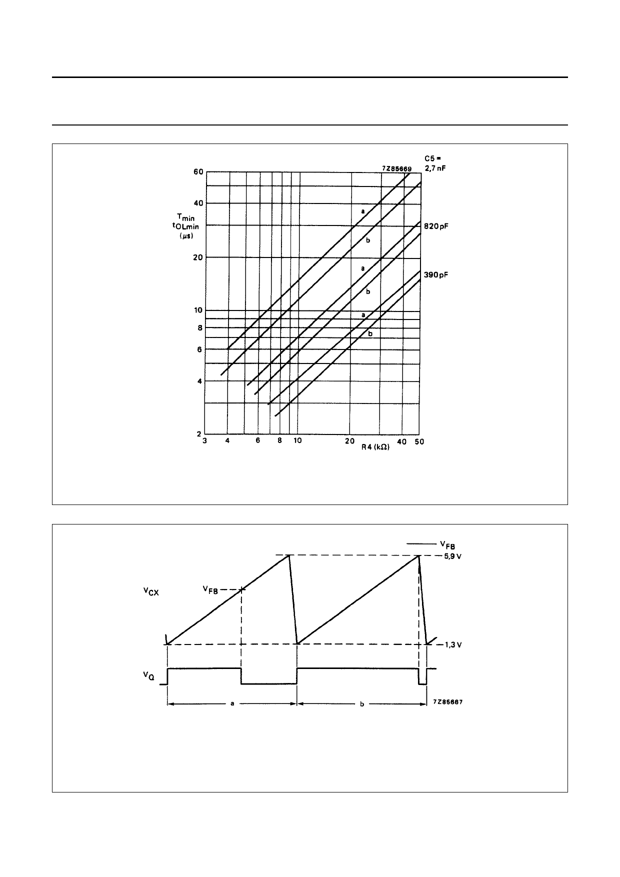
Fig.6 Minimum output pulse repetition time Tmin (curves a) and minimum output LOW time tOLmin (curves b) in
the frequency regulation mode as a function of external resistor R4 connected between RX and ground
with external capacitor C5 connected between CX and ground as a parameter.
Fig.7
Timing diagram for the duty factor regulation mode showing the voltage on external capacitor C5
connected between CX and ground and the output voltage as a function of time for two combinations of
input signals. a: The voltages on inputs FB or LIM are below 5,9 V. The circuit is in its normal regulation
range. b: The voltages on inputs FB and LIM are higher than 5,9 V. The circuit produces its minimum
output LOW time, giving the maximum duty factor of the SMPS.
August 1982
11
11 Page | ||
| Páginas | Total 16 Páginas | |
| PDF Descargar | [ Datasheet TEA1039.PDF ] | |
Hoja de datos destacado
| Número de pieza | Descripción | Fabricantes |
| TEA1039 | Control circuit for switched-mode power supply | NXP Semiconductors |
| Número de pieza | Descripción | Fabricantes |
| SLA6805M | High Voltage 3 phase Motor Driver IC. |
Sanken |
| SDC1742 | 12- and 14-Bit Hybrid Synchro / Resolver-to-Digital Converters. |
Analog Devices |
|
DataSheet.es es una pagina web que funciona como un repositorio de manuales o hoja de datos de muchos de los productos más populares, |
| DataSheet.es | 2020 | Privacy Policy | Contacto | Buscar |
