|
|
|
PDF TPC8107 Data sheet ( Hoja de datos )
| Número de pieza | TPC8107 | |
| Descripción | TOSHIBA Field Effect Transistor Silicon P Channel MOS Type (U-MOSIII) | |
| Fabricantes | Toshiba Semiconductor | |
| Logotipo | ||
Hay una vista previa y un enlace de descarga de TPC8107 (archivo pdf) en la parte inferior de esta página. Total 7 Páginas | ||
|
No Preview Available !
TPC8107
TOSHIBA Field Effect Transistor Silicon P Channel MOS Type (U-MOSIII)
TPC8107
Lithium Ion Battery Applications
Notebook PC Applications
Portable Equipment Applications
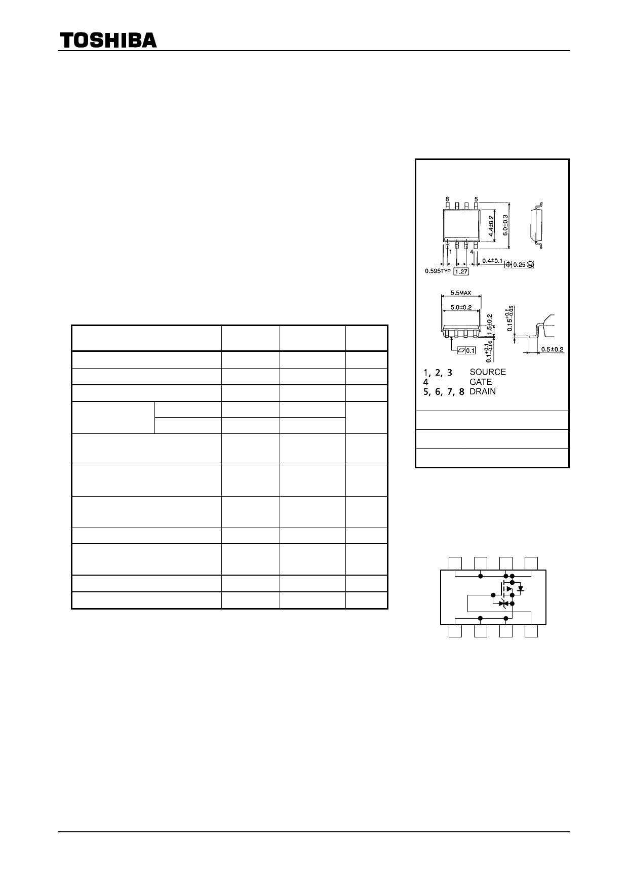
Unit: mm
· Small footprint due to small and thin package
· Low drain-source ON resistance: RDS (ON) = 5.5 mΩ (typ.)
· High forward transfer admittance: |Yfs| = 31 S (typ.)
· Low leakage current: IDSS = −10 µA (max) (VDS = −30 V)
· Enhancement-mode: Vth = −0.8 to −2.0 V (VDS = −10 V, ID = −1 mA)
Maximum Ratings (Ta = 25°C)
Characteristics
Symbol
Rating
Unit
Drain-source voltage
Drain-gate voltage (RGS = 20 kW)
Gate-source voltage
Drain current
DC (Note 1)
Pulse (Note 1)
Drain power dissipation
(t = 10 s)
(Note 2a)
Drain power dissipation
(t = 10 s)
(Note 2b)
Single pulse avalanche energy
(Note 3)
Avalanche current
Repetitive avalanche energy
(Note 2a) (Note 4)
Channel temperature
Storage temperature range
VDSS
VDGR
VGSS
ID
IDP
PD
PD
EAS
IAR
EAR
Tch
Tstg
-30
-30
±20
-13
-52
1.9
1.0
219
-13
0.19
150
-55 to 150
V
V
V
A
W
W
mJ
A
mJ
°C
°C
Note: For (Note 1), (Note 2), (Note 3) and (Note 4), please refer to the
next page.
This transistor is an electrostatic sensitive device. Please handle with
caution.
JEDEC
―
JEITA
―
TOSHIBA
2-6J1B
Weight: 0.080 g (typ.)
Circuit Configuration
8765
1234
1 2003-02-20
1 page 
RDS (ON) – Ta
30
Common source
Pulse test
20
ID = -13 A, -6.5 A, -3 A
10 VGS = -4 V
ID = -13 A, -6.5 A, -3 A
-10
0
-80 -40
0
40 80 120 160
Ambient temperature Ta (°C)
10000
3000
Capacitance – VDS
Ciss
1000
300
Coss
Crss
Common source
100 VGS = 0 V
f = 1 MHz
Ta = 25°C
30
-0.1 -0.3
-1
-3
-10 -30
Drain-source voltage VDS (V)
-100
TPC8107
-100
-10
IDR – VDS
-5 -3
-10
-1
VGS = 0 V
-1
-0.1
0
Common source
Ta = 25°C
Pulse test
0.2 0.4 0.6 0.8 1.0 1.2
Drain-source voltage VDS (V)
Vth – Ta
-2.0
Common source
VDS = -10 V
-1.6
ID = -1 mA
Pulse test
-1.2
-0.8
-0.4
0
-80 -40
0
40 80 120 160
Ambient temperature Ta (°C)
2.0
(1)
1.6
1.2
(2)
0.8
PD – Ta
(1) Device mounted on a
glass-epoxy board (a)
(Note 2a)
(2) Device mounted on a
glass-epoxy board (b)
(Note 2b)
t = 10 s
0.4
0
0 40 80 120 160 200
Ambient temperature Ta (°C)
Dynamic input/output characteristics
-30
Common source
VDD = -24 V
ID = -13 A
VDS
Ta = 25°C
Pulse test
-20
-30
-20
-12
-10
-6
0
0
-6
VDD = -24 V -10
-12
VGS
40 80 120 160
Total gate charge Qg (nC)
0
200
5 2003-02-20
5 Page | ||
| Páginas | Total 7 Páginas | |
| PDF Descargar | [ Datasheet TPC8107.PDF ] | |
Hoja de datos destacado
| Número de pieza | Descripción | Fabricantes |
| TPC8102 | TOSHIBA Field Effect Transistor Silicon P Channel MOS Type (MOSVI) | Toshiba Semiconductor |
| TPC8103 | Silicon P Channel MOS Type Field Effect Transistor | Toshiba Semiconductor |
| TPC8105-H | High Speed and High Efficiency DC-DC Converters | Toshiba Semiconductor |
| TPC8106-H | SILICON P CHANNEL MOS TYPE | Toshiba Semiconductor |
| Número de pieza | Descripción | Fabricantes |
| SLA6805M | High Voltage 3 phase Motor Driver IC. |
Sanken |
| SDC1742 | 12- and 14-Bit Hybrid Synchro / Resolver-to-Digital Converters. |
Analog Devices |
|
DataSheet.es es una pagina web que funciona como un repositorio de manuales o hoja de datos de muchos de los productos más populares, |
| DataSheet.es | 2020 | Privacy Policy | Contacto | Buscar |