|
|
PDF USBUF02W6 Data sheet ( Hoja de datos )
| Número de pieza | USBUF02W6 | |
| Descripción | EMI FILTER AND LINE TERMINATION FOR USB UPSTREAM PORTS | |
| Fabricantes | STMicroelectronics | |
| Logotipo |  |
|
Hay una vista previa y un enlace de descarga de USBUF02W6 (archivo pdf) en la parte inferior de esta página. Total 9 Páginas | ||
|
No Preview Available !
®
A.S.D.™
USBUFxxW6
EMI FILTER AND LINE TERMINATION
FOR USB UPSTREAM PORTS
APPLICATIONS
EMI Filter and line termination for USB upstream
ports on:
- USB Hubs
- PC peripherals
FEATURES
s Monolithic device with recommended line termi-
nation for USB upstream ports
s Integrated Rt series termination and Ct bypass-
ing capacitors.
s Integrated ESD protection
s Small package size
DESCRIPTION
The USB specification requires upstream ports
to be terminated with pull-up resistors from the
D+ and D- lines to Vbus. On the
implementation of USB systems, the radiated
and conducted EMI should be kept within the
required levels as stated by the FCC
regulations. In addition to the requirements of
termination and EMC compatibility, the
computing devices are required to be tested for
ESD susceptibility.
The USBUFxxW6 provides the recommended line
termination while implementing a low pass filter to
limit EMI levels and providing ESD protection
which exceeds IEC61000-4-2 level 4 standard.
The device is packaged in a SOT323-6L which is
the smallest available lead frame package (50%
smaller than the standard SOT23).
BENEFITS
s EMI / RFI noise suppression
s Required line termination for USB upstream
ports
s ESD protection exceeding IEC61000-4-2 level 4
s High flexibility in the design of high density
boards
s Tailored to meet USB 1.1 standard
TM: ASD and TRANSIL are a trademarks of STMicroelectronics.
March 2002 - Ed: 3A
SOT323-6L
FUNCTIONAL DIAGRAM
3.3 V
Rt Rp
D1
Ct
Grd
Rt
D2
Ct
D4
3.3 V
D3
CODE 01
CODE 02
Tolerance
Rt
33Ω
22Ω
±10%
Rp
1.5kΩ
1.5kΩ
±10%
Ct
47pF
47pF
±20%
1/9
1 page 
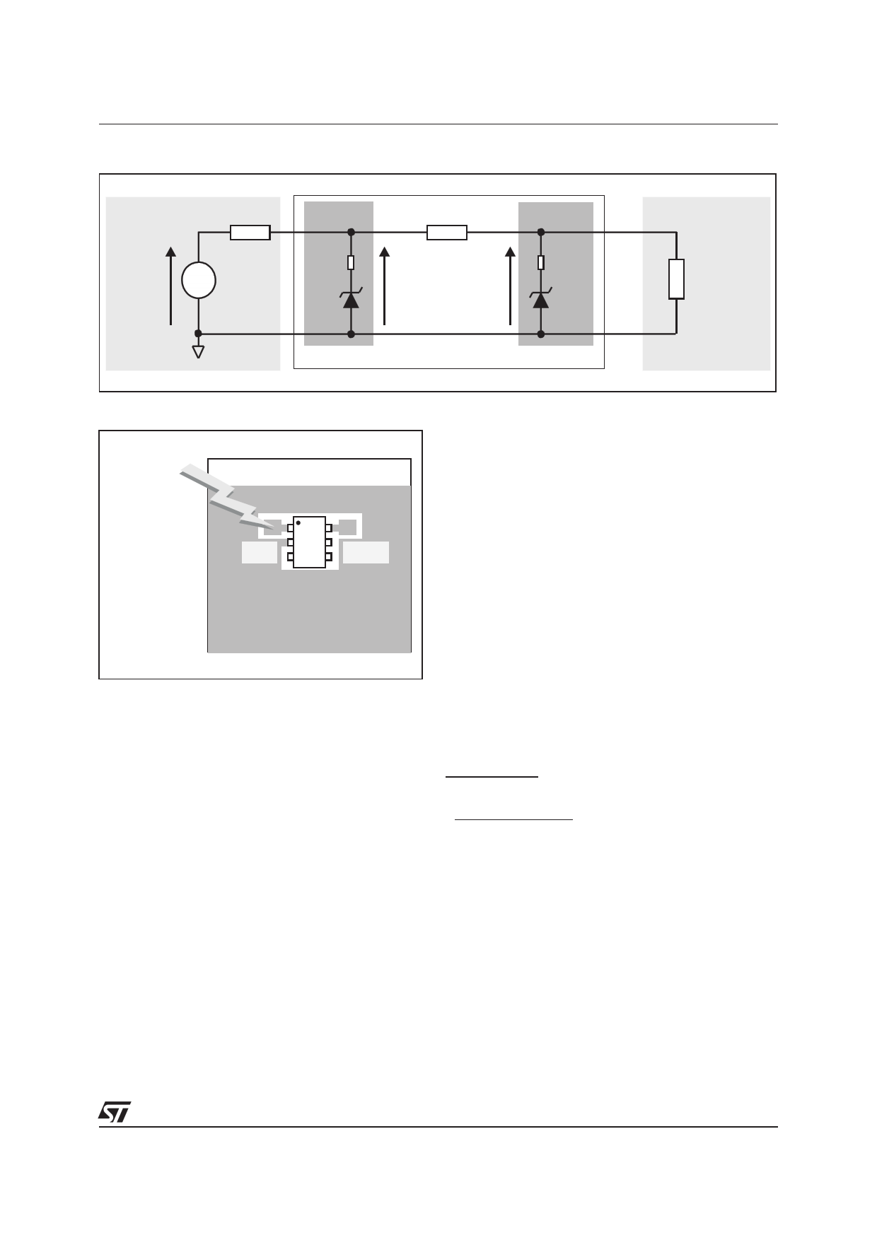
Fig. A5: USBUFxxW6 ESD clamping behavior
Rg S1 Rt S2
Rd Vinput
Rd
VPP
VBR
Voutput
VBR
ESD Surge
USBUF01W6
Fig. A6: Measurement board
ESD
SURGE
16kV
Air
Discharge
TEST BOARD
Vin Vout
USBUFxxW6
Rload
Device
to be
protected
To have a good approximation of the remaining voltages at both Vin and Vout stages, we give the typical
dynamical resistance value Rd. By taking into account these following hypothesis : Rt>Rd, Rg>Rd and
Rload>Rd, it gives these formulas:
Vinput = Rg.VBR + Rd.Vg
Rg
Voutput = Rt.VBR + Rd.Vinput
Rt
The results of the calculation done for Vg=8kV, Rg=330Ω (IEC61000-4-2 standard), VBR=7V (typ.)
and Rd = 1Ω (typ.) give:
Vinput = 31.2 V
Voutput = 7.95 V
This confirms the very low remaining voltage across the device to be protected. It is also important to note
that in this approximation the parasitic inductance effect was not taken into account. This could be few
tenths of volts during few ns at the Vinput side. This parasitic effect is not present at the Voutput side due
the low current involved after the resistance Rt.
The measurements done hereafter show very clearly (Fig. A7) the high efficiency of the ESD protection :
- no influence of the parasitic inductances on Voutput stage
- Voutput clamping voltage very close to VBR (breakdown voltage) in the positive way
and -VF (forward voltage) in the negative way
5/9
5 Page | ||
| Páginas | Total 9 Páginas | |
| PDF Descargar | [ Datasheet USBUF02W6.PDF ] | |
Hoja de datos destacado
| Número de pieza | Descripción | Fabricantes |
| USBUF02W6 | EMI FILTER AND LINE TERMINATION FOR USB UPSTREAM PORTS | STMicroelectronics |
| Número de pieza | Descripción | Fabricantes |
| SLA6805M | High Voltage 3 phase Motor Driver IC. |
Sanken |
| SDC1742 | 12- and 14-Bit Hybrid Synchro / Resolver-to-Digital Converters. |
Analog Devices |
|
DataSheet.es es una pagina web que funciona como un repositorio de manuales o hoja de datos de muchos de los productos más populares, |
| DataSheet.es | 2020 | Privacy Policy | Contacto | Buscar |
