|
|
|
PDF US3011CW Data sheet ( Hoja de datos )
| Número de pieza | US3011CW | |
| Descripción | 5 BIT PROGRAMMABLE SYNCHRONOUS BUCK CONTROLLER IC | |
| Fabricantes | UNISEM | |
| Logotipo | ||
Hay una vista previa y un enlace de descarga de US3011CW (archivo pdf) en la parte inferior de esta página. Total 11 Páginas | ||
|
No Preview Available !
US3011
5 BIT PROGRAMMABLE SYNCHRONOUS BUCK
FEATURES
CONTROLLER IC
PRELIMINARY DATASHEET
DESCRIPTION
Dual Layout Compatible with HIP6004A
Designed to meet Intel specification of VRM8.4
for Pentium III™
On board DAC programs the output voltage
from 1.3V to 3.5V. The US3011 remains on for
VID code of (11111).
Loss less Short Circuit Protection
Synchronous operation allows maximum
efficiency
Patented architecture allows fixed frequency
operation as well as 100% duty cycle during
dynamic load
Over Voltage Protection Output
Soft Start
High current totem pole driver for direct
driving of the external Power MOSFET
Power Good function
APPLICATIONS
Pentium III & Pentium II™ processor DC to DC con-
verter application
Low cost Pentium with AGP
The US3011controller IC is specifically designed to meet
Intel specification for latest Pentium III™ microproces-
sor applications as well as the next generation P6 fam-
ily processors. These products feature a patented topol-
ogy that in combination with a few external components
as shown in the typical application circuit ,will provide in
excess of 20A of output current for an on- board DC/DC
converter while automatically providing the right output
voltage via the 5 bit internal DAC.These devices also
features, loss less current sensing by using the Rds-
on of the high side Power MOSFET as the sensing
resistor, a Power Good window comparator that switches
its open collector output low when the output is outside
of a ±10% window and an OVP output. Other features of
the device are ; Undervoltage lockout for both 5V and
12V supplies , an external programmable soft start func-
tion as well as programming the oscillator frequency by
using an external capacitor.
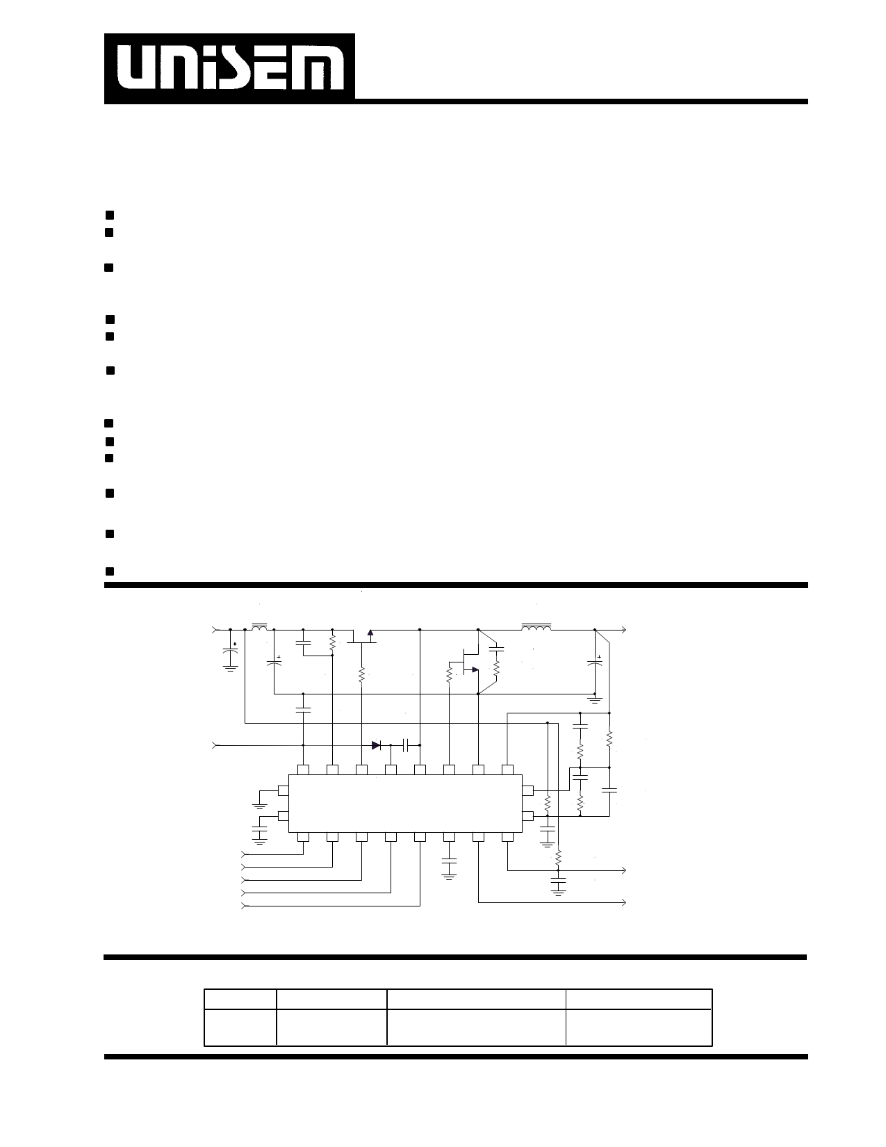
TYPICAL APPLICATION
L1
5V
C5 R1
C1
C3
Q1
R2
L2
C8
Q2
R4
R3
C10
12V
C2
VID4
VID3
VID2
VID1
VID0
C6
D1 C4
18 2
V12 CS+
11 NC/Gnd
3 SS
D4
8
D3
7
14
HDrv
D2
6
15
NC/
Boot
13
CS-
US3011
D1 D0
54
17
LDrv
Ct/Rt
20
16 1
Gnd NC/Sen
Vfb 10
R5
V5/Comp 9
OVP
19
PGd
12
C9
C7
C11
R7
R9
C12
R8
C13
R6
C14
3011app1-1.1
Power Good
OVP
Notes: Pentium II and Pentium III are
trade marks of Intel Corp.
PACKAGE ORDER INFORMATION
Ta (°C) Device
0 TO 70 US3011CW
Package
20 pin Plastic SOIC WB
VID Voltage Range
1.3V to 3.5V
Rev. 1.3
12/8/00
4-1
1 page 
BLOCK DIAGRAM
US3011
V12
V5
D0
D1
D2
D3
D4
Enable
UVLO
Vset
Enable
5Bit
DAC,
Ctrl
Logic
OVP
1.18Vset
Vset
+
Slope
Comp
Enable
PWM
Control
Osc
V12
V12
Soft
Start &
Fault
Logic
Enable
Over
Current
200uA
1.1Vset
Vfb
HDrv
LDrv
CS-
CS+
Ct
SS
PGd
Gnd
0.9Vset
3011Ablk1-1.1
Figure 1 - Simplified block diagram of the US3011.
Rev. 1.3
12/8/00
4-5
5 Page 
US3011
Layout Considerations
Switching regulators require careful attention to the lay-
out of the components, specifically power components
since they switch large currents. These switching com-
ponents can create large amount of voltage spikes and
high frequency harmonics if some of the critical compo-
nents are far away from each other and are connected
with inductive traces. The following is a guideline of how
to place the critical components and the connections
between them in order to minimize the above issues.
Start the layout by first placing the power components:
c) Q2 drain to L2
d) L2 to the output capacitors, C10
e) C10 to the slot 1
f) Input filter L1 to the C3
Connect the rest of the components using the shortest
connection possible
1) Place the input capacitors C3 and the high side
mosfet ,Q1 as close to each other as possible
2) Place the synchronous mosfet,Q2 and the Q1 as
close to each other as possible with the intention that
the source of Q1 and drain of the Q2 has the shortest
length.
3) Place the snubber R4 & C7 between Q1 & Q2.
4) Place the output inductor ,L2 and the output capaci-
tors ,C10 between the mosfet and the load with output
capacitors distributed along the slot 1 and close to it.
5) Place the bypass capacitors, C6 and C9 right next to
12V and 5V pins. C6 next to the 12V, pin 18 and C9
next to the 5V, pin 9.
6) Place the IC such that the pwm output drives, pins
14 and 17 are relatively short distance from gates of Q1
and Q2.
7) If the ouput voltage is to be adjusted, place resistor
dividers close to the feedback pin.
Note 1: Although, the device does not require resistor
dividers and the feedback pin can be directly connected
to the output, they can be used to set the outputs slightly
higher to account for any output drop at the load due to
the trace resistance. See the application note.
8) Place timing capacitor C7 close to pin20 and soft
start capacitor C2 close to pin 3.
Component connections:
Note : It is extremely important that no data bus
should be passing through the switching regulator
section specifically close to the fast transition nodes
such as PWM drives or the inductor voltage.
Using 4 layer board, dedicate on layer to GND, another
layer as the power layer for the 5V, 3.3V and Vcore.
Connect all grounds to the ground plane using di-
rect vias to the ground plane.
Use large low inductance/low impedance plane to con-
nect the following connections either using component
side or the solder side.
a) C3 to Q1 Drain
b) Q1 Source to Q2 Drain
Rev. 1.3
12/8/00
4-11
11 Page | ||
| Páginas | Total 11 Páginas | |
| PDF Descargar | [ Datasheet US3011CW.PDF ] | |
Hoja de datos destacado
| Número de pieza | Descripción | Fabricantes |
| US3011CW | 5 BIT PROGRAMMABLE SYNCHRONOUS BUCK CONTROLLER IC | UNISEM |
| Número de pieza | Descripción | Fabricantes |
| SLA6805M | High Voltage 3 phase Motor Driver IC. |
Sanken |
| SDC1742 | 12- and 14-Bit Hybrid Synchro / Resolver-to-Digital Converters. |
Analog Devices |
|
DataSheet.es es una pagina web que funciona como un repositorio de manuales o hoja de datos de muchos de los productos más populares, |
| DataSheet.es | 2020 | Privacy Policy | Contacto | Buscar |