|
|
|
PDF IRFB41N15D Data sheet ( Hoja de datos )
| Número de pieza | IRFB41N15D | |
| Descripción | Power MOSFET(Vdss=150V/ Rds(on)max=0.045ohm/ Id=41A) | |
| Fabricantes | International Rectifier | |
| Logotipo | ||
Hay una vista previa y un enlace de descarga de IRFB41N15D (archivo pdf) en la parte inferior de esta página. Total 11 Páginas | ||
|
No Preview Available !
SMPS MOSFET
PD- 93804A
IRFB41N15D
IRFS41N15D
IRFSL41N15D
HEXFET® Power MOSFET
Applications
l High frequency DC-DC converters
VDSS
150V
RDS(on) max
0.045Ω
ID
41A
Benefits
l Low Gate-to-Drain Charge to Reduce
Switching Losses
l Fully Characterized Capacitance Including
Effective COSS to Simplify Design, (See
App. Note AN1001)
l Fully Characterized Avalanche Voltage
and Current
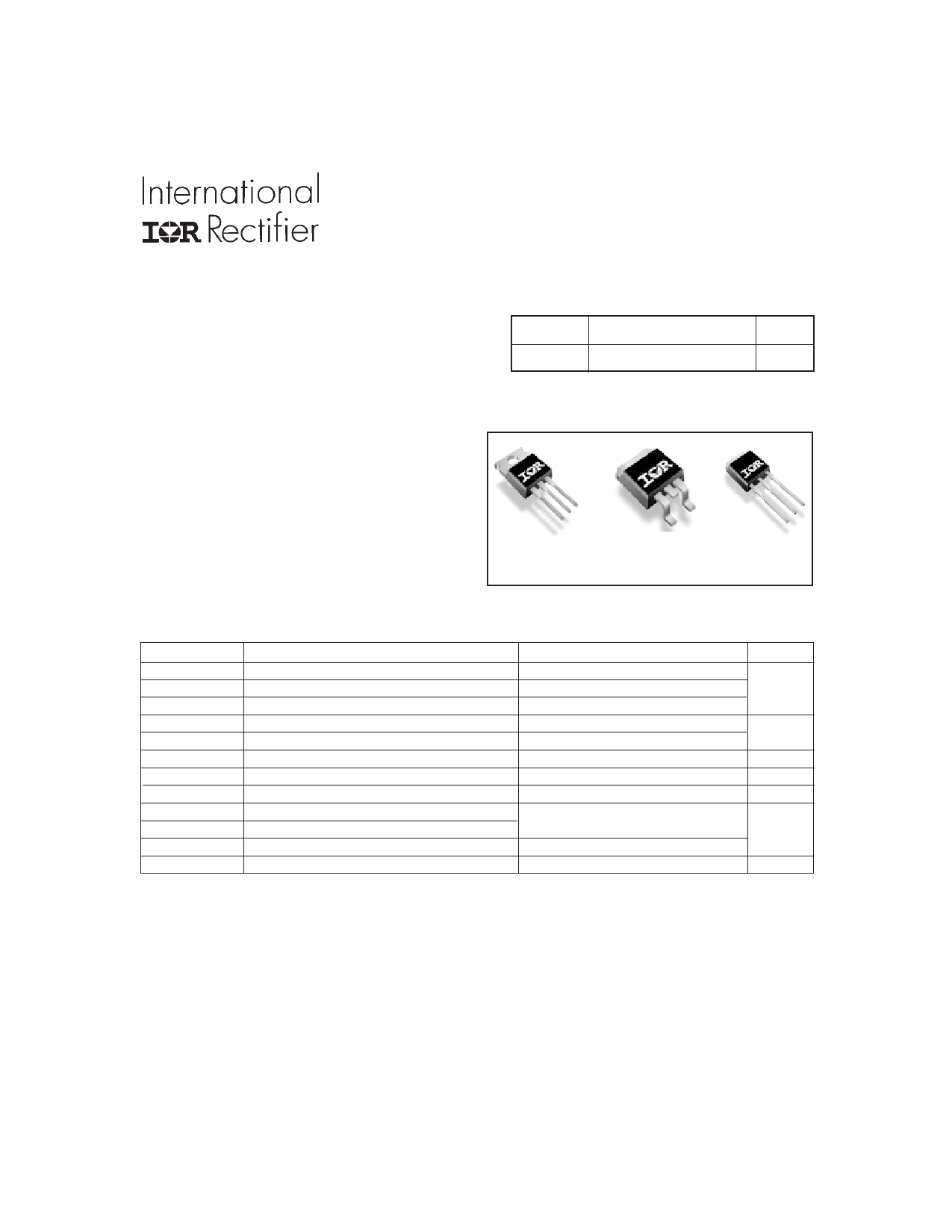
TO-220AB
IRFB41N15D
D2Pak
TO-262
IRFS41N15D IRFSL41N15D
Absolute Maximum Ratings
ID @ TC = 25°C
ID @ TC = 100°C
IDM
PD @TA = 25°C
PD @TC = 25°C
VGS
dv/dt
TJ
TSTG
Parameter
Continuous Drain Current, VGS @ 10V
Continuous Drain Current, VGS @ 10V
Pulsed Drain Current
Power Dissipation
Power Dissipation
Linear Derating Factor
Gate-to-Source Voltage
Peak Diode Recovery dv/dt
Operating Junction and
Storage Temperature Range
Soldering Temperature, for 10 seconds
Mounting torqe, 6-32 or M3 screw
Max.
41
29
164
3.1
200
1.3
± 30
2.7
-55 to + 175
300 (1.6mm from case )
10 lbf•in (1.1N•m)
Units
A
W
W/°C
V
V/ns
°C
Typical SMPS Topologies
l Telecom 48V input DC-DC Active Clamp Reset Forward Converter
Notes through
are on page 11
www.irf.com
1
2/14/00
1 page 
IRFB/IRFS/IRFSL41N15D
50
40
30
20
10
0
25 50 75 100 125 150 175
TC , Case Temperature ( °C)
Fig 9. Maximum Drain Current Vs.
Case Temperature
10
VDS
VGS
RG
RD
D.U.T.
VGS
Pulse Width ≤ 1 µs
Duty Factor ≤ 0.1 %
+-VDD
Fig 10a. Switching Time Test Circuit
VDS
90%
10%
VGS
td(on) tr
td(off) tf
Fig 10b. Switching Time Waveforms
1
D = 0.50
0.20
0.1 0.10
0.05
0.02
0.01
0.01
0.00001
PDM
t1
t2
SINGLE PULSE
(THERMAL RESPONSE)
Notes:
1. Duty factor D = t1 / t 2
2. Peak T J = P DM x Z thJC + TC
0.0001
0.001
0.01
t1 , Rectangular Pulse Duration (sec)
0.1
Fig 11. Maximum Effective Transient Thermal Impedance, Junction-to-Case
www.irf.com
1
5
5 Page 
IRFB/IRFS/IRFSL41N15D
D2Pak Tape & Reel Information
TR R
1 .6 0 (.0 6 3 )
1 .5 0 (.0 5 9 )
4 .1 0 (.1 6 1 )
3 .9 0 (.1 5 3 )
F E E D D IR E C TIO N 1 .8 5 (.0 7 3 )
1 .6 5 (.0 6 5 )
TRL
10.90 (.429)
10.70 (.421)
1 .6 0 (.0 6 3 )
1 .5 0 (.0 5 9 )
11.60 (.457)
11.40 (.449)
15.42 (.609)
15.22 (.601)
1.75 (.069)
1.25 (.049)
16.10 (.634)
15.90 (.626)
0.368 (.0145)
0.342 (.0135)
2 4 .3 0 (.9 5 7 )
2 3 .9 0 (.9 4 1 )
4 .7 2 (.1 3 6)
4 .5 2 (.1 7 8)
FEED DIRECTION
13.50 (.532)
12.80 (.504)
2 7.4 0 (1.079 )
2 3.9 0 (.9 41)
4
330.00
(14.173)
MAX.
6 0.0 0 (2.36 2)
M IN .
Notes:
NO TES :
1 . CO M F OR M S TO E IA -418 .
2 . CO N TR O L LIN G D IM E N SIO N : M IL LIM E T ER .
3 . DIM E NS IO N M EA S UR E D @ H U B.
4 . IN C LU D ES FL AN G E DIST O R T IO N @ O UT E R E D G E.
26.40 (1.039)
24.40 (.961)
3
30.40 (1.197)
MAX.
4
Repetitive rating; pulse width limited by
max. junction temperature.
Pulse width ≤ 300µs; duty cycle ≤ 2%.
Starting TJ = 25°C, L = 1.5mH
RG = 25Ω, IAS = 25A.
Coss eff. is a fixed capacitance that gives the same charging time
as Coss while VDS is rising from 0 to 80% VDSS
ISD ≤ 25A, di/dt ≤ 340A/µs, VDD ≤ V(BR)DSS,
This is only applied to TO-220AB package
TJ ≤ 175°C
This is applied to D2Pak, when mounted on 1" square PCB ( FR-4 or G-10 Material ).
For recommended footprint and soldering techniques refer to application note #AN-994.
WORLD HEADQUARTERS: 233 Kansas St., El Segundo, California 90245, Tel: (310) 252-7105
IR GREAT BRITAIN: Hurst Green, Oxted, Surrey RH8 9BB, UK Tel: ++ 44 1883 732020
IR CANADA: 15 Lincoln Court, Brampton, Ontario L6T3Z2, Tel: (905) 453 2200
IR GERMANY: Saalburgstrasse 157, 61350 Bad Homburg Tel: ++ 49 6172 96590
IR ITALY: Via Liguria 49, 10071 Borgaro, Torino Tel: ++ 39 11 451 0111
IR JAPAN: K&H Bldg., 2F, 30-4 Nishi-Ikebukuro 3-Chome, Toshima-Ku, Tokyo Japan 171 Tel: 81 3 3983 0086
IR SOUTHEAST ASIA: 1 Kim Seng Promenade, Great World City West Tower, 13-11, Singapore 237994 Tel: ++ 65 838 4630
IR TAIWAN:16 Fl. Suite D. 207, Sec. 2, Tun Haw South Road, Taipei, 10673, Taiwan Tel: 886-2-2377-9936
Data and specifications subject to change without notice. 02/2000
www.irf.com
11
11 Page | ||
| Páginas | Total 11 Páginas | |
| PDF Descargar | [ Datasheet IRFB41N15D.PDF ] | |
Hoja de datos destacado
| Número de pieza | Descripción | Fabricantes |
| IRFB41N15D | Power MOSFET(Vdss=150V/ Rds(on)max=0.045ohm/ Id=41A) | International Rectifier |
| IRFB41N15DPBF | HEXFET Power MOSFET | International Rectifier |
| Número de pieza | Descripción | Fabricantes |
| SLA6805M | High Voltage 3 phase Motor Driver IC. |
Sanken |
| SDC1742 | 12- and 14-Bit Hybrid Synchro / Resolver-to-Digital Converters. |
Analog Devices |
|
DataSheet.es es una pagina web que funciona como un repositorio de manuales o hoja de datos de muchos de los productos más populares, |
| DataSheet.es | 2020 | Privacy Policy | Contacto | Buscar |