|
|
|
PDF SL4052B Data sheet ( Hoja de datos )
| Número de pieza | SL4052B | |
| Descripción | Analog Multiplexer Demultiplexer High-Performance Silicon-Gate CMOS | |
| Fabricantes | System Logic Semiconductor | |
| Logotipo | ||
Hay una vista previa y un enlace de descarga de SL4052B (archivo pdf) en la parte inferior de esta página. Total 6 Páginas | ||
|
No Preview Available !
SL4052B
Analog Multiplexer Demultiplexer
High-Performance Silicon-Gate CMOS
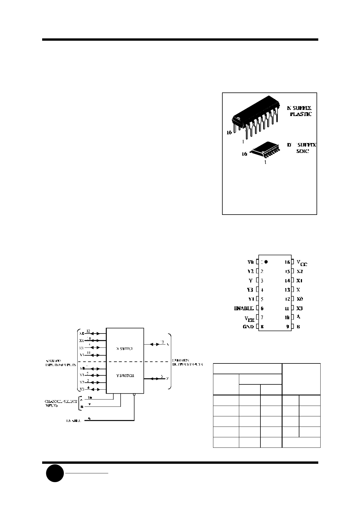
The SL4052B analog multiplexer/demultiplexer is digitally controlled
analog switches having low ON impedance and very low OFF leakage
current. Control of analog signals up to 20V peak-to-peak can be
achieved by digital signal amplitudes of 4.5 to 20V (if VCC - GND = 3V, a
VCC - VEE of up to 13 V can be controlled; for VCC - VEE level differences
above 13V a VCC - GND of at least 4.5V is required).
These multiplexer circuits dissipate extremely low quiescent power
over the full VCC -GND and VCC - VEE supply-voltage ranges,
independent of the logic state of the control signals. When a logic
“1”is present at the ENABLE input terminal all channels are off.
The SL4052 is a differential 4-channel multiplexer having two binary
control inputs. A and B, and an enable input. The two binary input
signals select 1 of 4 pairs of channels to turned on and connect the
analog inputs to the outputs.
• Operating Voltage Range: 3.0 to 18 V
• Maximum input current of 1
µA at 18 V over full package-temperature range; 100 nA at 18 V and
25°C
• Noise margin (over full package temperature range):
1.0 V min @ 5.0 V supply
2.0 V min @ 10.0 V supply
2.5 V min @ 15.0 V supply
ORDERING INFORMATION
SL4052BN Plastic
SL4052BD SOIC
TA = -55° to 125° C for all packages
PIN ASSIGNMENT
LOGIC DIAGRAM
Double-Pole, 4-Position
Plus Common Off
PIN 16 =VCC
PIN 7 = VEE
PIN 8 = GND
SLS
System Logic
Semiconductor
FUNCTION TABLE
Control Inputs
Enable
Select
BA
L LL
L LH
L HL
L HH
HX
X = don’t care
X
ON
Channels
Y0 X0
Y1 X1
Y2 X2
Y3 X3
None
1 page 
SL4052B
ADDITIONAL APPLICATION CHARACTERISTICS
Symbol
BW
THD
Parameter
Maximum On-
Channel
Bandwidth or
Minimum
Frequency
Response (-3db)
(-40db)
Feedthrough
Frequency (All
Channels OFF)
(-40db)
Signal Crosstalk
Frequency
Total Harmonic
Distortion
Test Conditions
VEE=GND
RL=1kΩ
20 log(VOS/VIS)=-3db
VOS at Common OUT/IN
VOS at Any Channel
VEE=GND
RL=1kΩ
20 log(VOS/VIS)=-40db
VOS at Common OUT/IN
VOS at Any Channel
VEE=GND
RL=1kΩ
20 log(VOS/VIS)=-40db
Between Sections :
Measured on Common
Measured on Any Chanel
VEE=GND
fIS=1kHz sine wave
- Address-or
VEE=GND
Enable to Signal RL=10kΩ**
Crosstalk
tr,tf=20ns
Square Wave
* Peak-to-peak voltage symmetrical about (VDD-VEE)/2
** Both ends of channel
VCC VIS Limit*
V V 25 °C Unit
10 5*
25 MHz
10 5*
60
10 5*
10 5*
10
8
6
10
5 2* 0.3 %
10 3* 0.2
15 5* 012
10 - 65 mv
(peak)
SLS
System Logic
Semiconductor
5 Page | ||
| Páginas | Total 6 Páginas | |
| PDF Descargar | [ Datasheet SL4052B.PDF ] | |
Hoja de datos destacado
| Número de pieza | Descripción | Fabricantes |
| SL4052B | Analog Multiplexer Demultiplexer High-Performance Silicon-Gate CMOS | System Logic Semiconductor |
| SL4052BD | Analog Multiplexer Demultiplexer High-Performance Silicon-Gate CMOS | System Logic Semiconductor |
| SL4052BN | Analog Multiplexer Demultiplexer High-Performance Silicon-Gate CMOS | System Logic Semiconductor |
| Número de pieza | Descripción | Fabricantes |
| SLA6805M | High Voltage 3 phase Motor Driver IC. |
Sanken |
| SDC1742 | 12- and 14-Bit Hybrid Synchro / Resolver-to-Digital Converters. |
Analog Devices |
|
DataSheet.es es una pagina web que funciona como un repositorio de manuales o hoja de datos de muchos de los productos más populares, |
| DataSheet.es | 2020 | Privacy Policy | Contacto | Buscar |