|
|
|
PDF SL4034B Data sheet ( Hoja de datos )
| Número de pieza | SL4034B | |
| Descripción | 8-Stage Static Bidirectional Parallel/ Serial Input/Output Bus Register | |
| Fabricantes | System Logic Semiconductor | |
| Logotipo | ||
Hay una vista previa y un enlace de descarga de SL4034B (archivo pdf) en la parte inferior de esta página. Total 9 Páginas | ||
|
No Preview Available !
SL4034B
8-Stage Static Bidirectional Parallel/
Serial Input/Output Bus Register
High-Voltage Silicon-Gate CMOS
The SL4034B is a static eight-stage parallel-or serial-input parallel-
output register. It can be used to:
1) bidirectionally transfer parallel information between two buses, 2)
convert serial data to parallel form and direct the parallel data to either
of two buses, 3) store (recirculate) parallel data, or 4) accept parallel
data from either of two buses and convert that data to serial form.
Inputs that control the operations include a single-phase CLOCK (CL),
A DATA ENABLE (AE), ASYNCHRONOUS/SYNCHRONOUS (A/S),
A-BUS-TO-B-BUS/ B-BUS-TO-A-BUS (A/B), and PARALLEL/SERIAL
(P/S).
Data inputs include 16 bidirectional parallel data lines of which the
eight A data lines are inputs (3-state outputs) and the B data lines are
outputs (inputs) dependung on the signal level on the A/B input. In
addition, an input for SERIAL DATA is also provided.
All register stages are D-type master-slave flip-flops with
separate master and slave clock inputs generated internally to allow
synchronous or asynchronous data transfer from master to slave.
• Operating Voltage Range: 3.0 to 18 V
• Maximum input current of 1 µA at 18 V over full package-
temperature range; 100 nA at 18 V and 25°C
• Noise margin (over full package temperature range):
1.0 V min @ 5.0 V supply
2.0 V min @ 10.0 V supply
2.5 V min @ 15.0 V supply
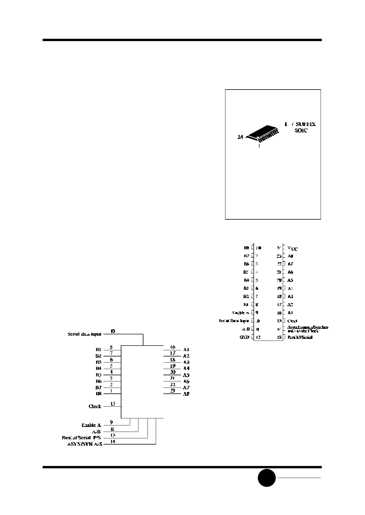
LOGIC DIAGRAM
ORDERING INFORMATION
SL4034BD SOIC
TA = -55° to 125° C
for package
PIN ASSIGNMENT
PIN 24=VCC
PIN 12= GND
SLS
System Logic
Semiconductor
1 page 
SL4034B
TRUTH TABLE FOR REGISTER INPUT-LEVELS AND RESULTING REGISTER
OPERATION
“A”
Enable P/S A/B A/S
Operation*
L L L X Serial Mode; Synch. Serial Data Input, “A” Parallel Data Outputs Disabled
L L H X Serial Mode, Synch. Serial Data Input, “B” Parallel Data Output
L H L L Parallel Mode; “B” Synch. Parallel Data Inputs, “A” Parallel Data Outputs
Disabled
L H L H Parallel Mode; “B” Asynch. Parallel Data Inputs, “A” Parallel Data Outputs
Disabled
L H H L Parallel Mode; “A” Parallel Data Inputs Disabled, “B” Parallel Data Outputs,
Synch. Data Recirculation
L H H H Parallel Mode; “A” Parallel Data Inputs Disabled, “B” Parallel Data Outputs,
Asynch. Data Recirculation
H L L X Serial Mode; Synch. Serial Data Input, “A” Parallel Data Output
H L H X Serial Mode; Synch. Serial Data Input, “B” Parallel Data Output
H H L L Parallel Mode; “B” Synch. Parallel Data Input, “A” Parallel Data Output
H H L H Parallel Mode; “B” Asynch. Parallel Data Input, “A” Parallel Data Output
H H H L Parallel Mode; “A” Synch. Parallel Data Input, “B” Parallel Data Output
H H H H Parallel Mode; “A” Asynch. Parallel Data Input, “B” Parallel Data Output
* Outputs change at positive transition of clock in the serial mode and when the A/S control input is “low”
in the parallel mode. During transfer from parallel to serial operation A/S should remain low in oder to prevent DS
transfer into Flip Flops.
X = Don’t Care
PARALLEL OPERATION
A high P/S input signal allows data transfer into the register via the parallel data lines synchronously with
the positive transition of the clock provided the A/S input is low. If the A/S input is high the transfer is
independent of the clock. The direction of data flow is controlled by the A/B input. When this signal is high the
A data lines are inputs (and B data lines are outputs); a low A/B signal reverses the direction of data flow.
The AE input is an additional feature which allows many registers to feed data to a common bus. The A
DATA lines are enabled only when this signal is high.
Data storage through recirculation of data in each register stage is accomplished by making the A/B signal
high and the AE signal low.
SERIAL OPERATION
A low P/S signal allows serial data to transfer into the register synchronously with the positive transition of
the clock. The A/S input is internally disabled when the register is in the serial mode (asynchronous serial
operation is not allowed).
The serial data appears as output data on either the B lines (when A/B is high) or the A lines (when A/B is
low and the AE signal is high).
SLS
System Logic
Semiconductor
5 Page | ||
| Páginas | Total 9 Páginas | |
| PDF Descargar | [ Datasheet SL4034B.PDF ] | |
Hoja de datos destacado
| Número de pieza | Descripción | Fabricantes |
| SL4034B | 8-Stage Static Bidirectional Parallel/ Serial Input/Output Bus Register | System Logic Semiconductor |
| SL4034BD | 8-Stage Static Bidirectional Parallel/ Serial Input/Output Bus Register | System Logic Semiconductor |
| Número de pieza | Descripción | Fabricantes |
| SLA6805M | High Voltage 3 phase Motor Driver IC. |
Sanken |
| SDC1742 | 12- and 14-Bit Hybrid Synchro / Resolver-to-Digital Converters. |
Analog Devices |
|
DataSheet.es es una pagina web que funciona como un repositorio de manuales o hoja de datos de muchos de los productos más populares, |
| DataSheet.es | 2020 | Privacy Policy | Contacto | Buscar |