|
|
PDF ISL6550A Data sheet ( Hoja de datos )
| Número de pieza | ISL6550A | |
| Descripción | SAM Supervisor And Monitor | |
| Fabricantes | Intersil Corporation | |
| Logotipo |  |
|
Hay una vista previa y un enlace de descarga de ISL6550A (archivo pdf) en la parte inferior de esta página. Total 11 Páginas | ||
|
No Preview Available !
®
Data Sheet
ISL6550A, ISL6550B, ISL6550C
July 2003
FN9036.2
SAM (Supervisor And Monitor)
The ISL6550 is a precision, flexible, VID-code-controlled
reference and voltage monitor for high-end microprocessor
and memory power supplies. It monitors various input
signals, and supervises the system (typically a DC/DC
converter) with its output signals. See the Block Diagram for
reference.
The ISL6550 includes a 5-bit DAC (Digital-to-Analog
Converter), which is programmed by the five VID inputs. The
voltage range of the BDAC (Buffered DAC output) is
determined by the DACHI and DACLO voltage levels, which
are externally adjustable through the R1, R2, R3 resistor
divider network. VREF5 is a precision-trimmed 5V reference,
and is used to set the voltage at the top of the resistor
divider.
Programmable window comparators monitor Over-Voltage
(OV) and Under-Voltage (UV) levels. The OVUVSEN input,
usually coming from the associated power converter device
is monitored and compared with BDAC; an error band is
established via the R4 and R5 resistor setting on the
OVUVTH pin. An optional external capacitor on the UVDLY
pin gives a programmable delay on the UV. A high gain
operational amplifier is available at pins VOPP, VOPM, and
VOPOUT; it can be used as a gain stage to permit
monitoring voltages that are different from the BDAC levels.
The PEN (Power supply ENable) input, driven from an open-
collector source, enables (when logic high) the external
converter output, via the PGOOD or START outputs (both
open-drain). They both basically indicate that the power
supply is enabled (PEN = high) and there are no fault
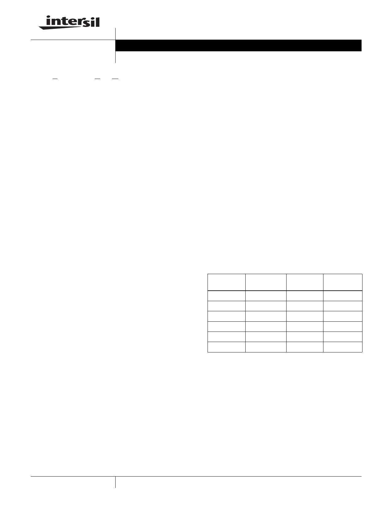
conditions. There are three logic options available, which
determine the START and PGOOD states; see the block
diagram or the Logic Options Table for more detail. The
three logic options are identified with a suffix letter A, B, or C
in the ordering information.
Features
• 12V supply operation
• 5V reference output
• 5-bit digital-to-analog converter
• Programmable DAC Range, within 0.8–5.0V
• Programmable undervoltage and overvoltage thresholds,
and latched fault detection
• Optional delayed undervoltage (programmable with
external capacitor)
• Undervoltage lockout (power-on-reset)
• Status Indicators (START, PGOOD)
• Uncommitted operational amplifier
• Compatible with ISL6551 full bridge controller
• 20 Lead SOIC and 20 lead QFN (5x5) packages
Applications
• Power Supplies for High End Microprocessors and Servers
• Can be paired with the ISL6551 FBC for a complete full-
bridge 48V-input converter, or used independently
Ordering Information
PART
NUMBER
TEMP. RANGE
(oC) PACKAGE PKG. DWG. #
ISL6550AIB
-40 to 85 20 Lead SOIC M20.3
ISL6550BIB
-40 to 85 20 Lead SOIC M20.3
ISL6550CIB
-40 to 85 20 Lead SOIC M20.3
ISL6550AIR
-40 to 85 20 Lead QFN L20.5x5
ISL6550BIR
-40 to 85 20 Lead QFN L20.5x5
ISL6550CIR
-40 to 85 20 Lead QFN L20.5x5
NOTE: The same part numbers with a “-T” suffix are available as
Tape and Reel.
1 CAUTION: These devices are sensitive to electrostatic discharge; follow proper IC Handling Procedures.
1-888-INTERSIL or 321-724-7143 | Intersil (and design) is a registered trademark of Intersil Americas Inc.
Copyright © Intersil Americas Inc. 2003. All Rights Reserved.
All other trademarks mentioned are the property of their respective owners.
1 page 
ISL6550A, ISL6550B, ISL6550C
Absolute Maximum Ratings
Supply Voltage, VCC . . . . . . . . . . . . . . . . . . . . . . . . . . . . . . . . .+15V
Input, Output or I/O Voltage . . . . . . . . . . . GND -0.3V to VCC +0.3V
ESD Rating
Human Body Model (Per MIL-STD-883 Method 3015.7) . . . . .3kV
Machine Model (Per EIAJ ED-4701 Method C-111) . . . . . . .200V
Operating Conditions
Supply Voltage, VCC . . . . . . . . . . . . . . . . . . . . . . . . . . . +12V ±10%
Temperature Range. . . . . . . . . . . . . . . . . . . . . . . . . . -40oC to 85oC
Junction Temperature Range . . . . . . . . . . . . . . . . . -40oC to 125oC
Thermal Information
Thermal Resistance
θJA (oC/W) θJC (oC/W)
SOIC Package (Typical, Note 1) . . . . .
65
N/A
QFN Package (Typical, Note 2) . . . . . .
35
5
Maximum Junction Temperature (Plastic Package) . .
150
Maximum Storage Temperature Range . . . . . . . . . . . -65 to 150
Maximum Lead Temperature (Soldering 10s) . . . . . . .
300
(SOIC - Lead Tips Only)
For Recommended soldering conditions see Tech Brief TB389.
.
CAUTION: Stresses above those listed in “Absolute Maximum Ratings” may cause permanent damage to the device. This is a stress only rating and operation of the
device at these or any other conditions above those indicated in the operational sections of this specification is not implied.
NOTE:
1. θJA is measured with the component mounted on a high effective thermal conductivity test board in free air. See Tech Brief TB379 for details.
2. θJA is measured in free air with the component mounted on a high effective thermal conductivity test board with “direct attach” features. θJC, the
“case temp” is measured at the center of the exposed metal pad on the package underside. See Tech Brief TB379.
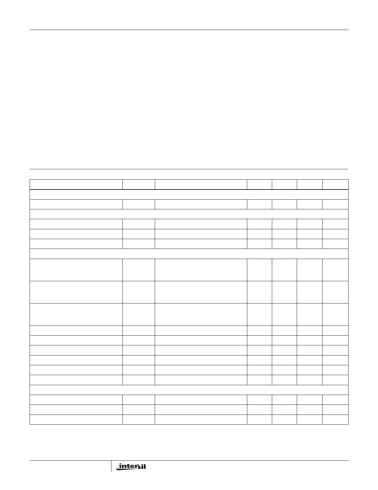
Electrical Specifications TA = 25oC, and VDD = 12V, unless otherwise specified
PARAMETER
SYMBOL
TEST CONDITIONS
SUPPLY CURRENT
Input Current
UNDER-VOLTAGE LOCKOUT
IIN VCC = 12V
VCC UVLO Turn-on Threshold
VCC UVLO Turn-off Threshold
VCC UVLO Threshold Hysteresis
DAC REFERENCE
DAC Output Error (See Notes 3, 4)
Step Size = 25mV
Vdaclo = 0.8V to 4.225V
Ibdac = 0.1mA to -1mA
DAC Output Error (See Notes 3, 4)
Step Size = 50mV
Vdaclo = 0.8V to 3.45V
Ibdac = 0.1mA to -1mA
DAC Output Error (See Notes 3, 4)
Step Size = 100mV
Vdaclo = 0.8V to 1.9V
Ibdac = 0.1mA to -1mA
VREF5 Voltage
VID0-VID4 Input LPUL (Vih)
VID0-VID4 Input MPDL (Vil)
VID0-VID4 Input Pull-Up Current
Vvidx = 0V
VID0-VID4 Input Leakage Current
Vvidx = 5V
Output Settling Time
±1LSB Error Band
UVDLY
Source Current
Sink Current
Threshold
MIN
TYP
MAX
UNITS
- 5 6 mA
9.2 9.4 9.9
8.2 8.4 8.9
- 1.0 -
-
-
-
-2 - +2 mV
-2 - +4 mV
-2 - +6 mV
4.95 - 5.05 V
2.0 - - V
- - 0.8 V
-15 -10 - mA
- - 1 µA
- - 20 µS
- -10 -
µA
- 10 - mA
-5- V
5
5 Page 
ISL6550A, ISL6550B, ISL6550C
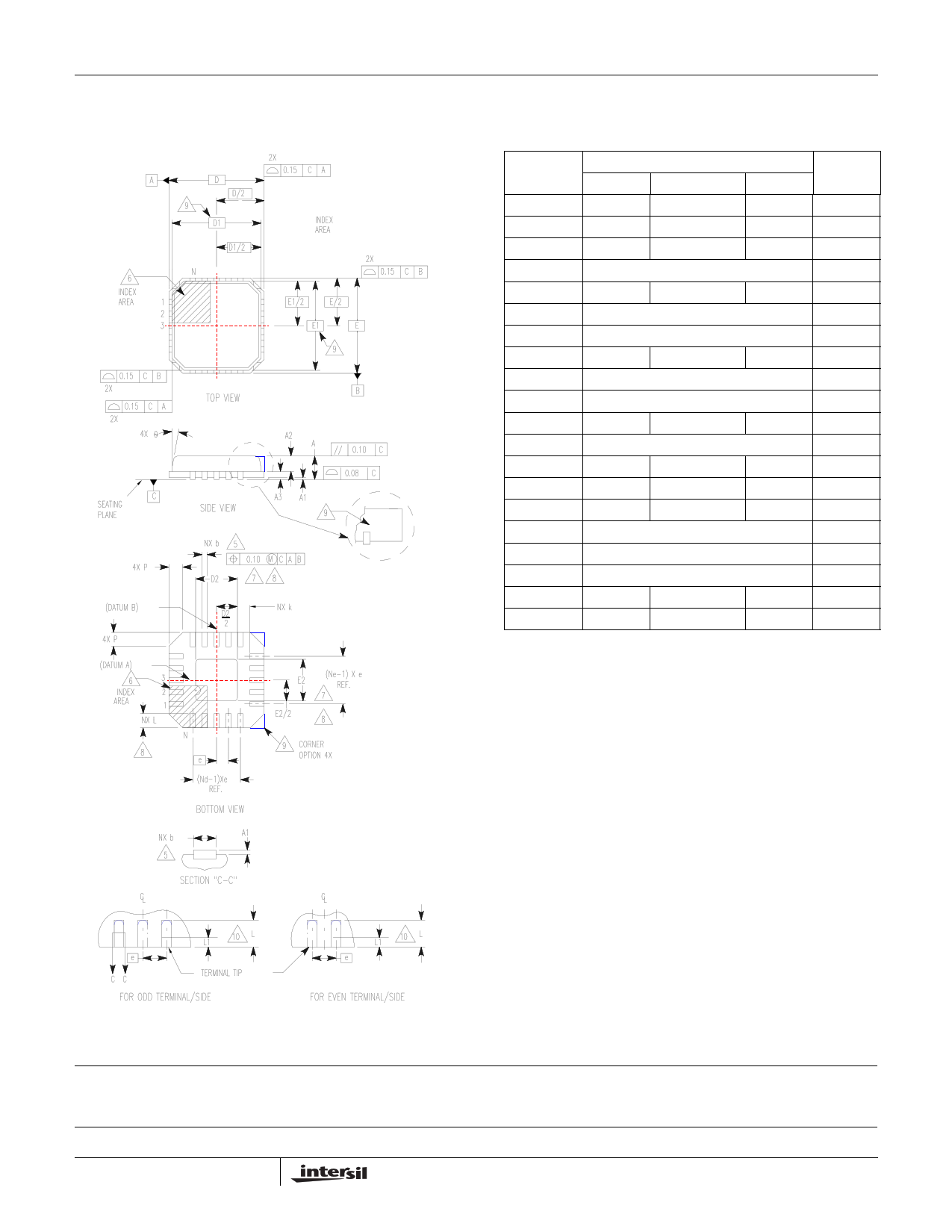
Quad Flat No-Lead Plastic Package (QFN)
Micro Lead Frame Plastic Package (MLFP)
L20.5x5
20 LEAD QUAD FLAT NO-LEAD PLASTIC PACKAGE
(COMPLIANT TO JEDEC MO-220VHHC ISSUE C)
SYMBOL
A
A1
A2
A3
b
D
D1
MILLIMETERS
MIN NOMINAL MAX
0.80 0.90 1.00
- - 0.05
- - 1.00
0.20 REF
0.23 0.28 0.38
5.00 BSC
4.75 BSC
NOTES
-
-
9
9
5, 8
-
9
D2 2.95 3.10 3.25 7, 8
E
5.00 BSC
-
E1 4.75 BSC 9
E2 2.95 3.10 3.25 7, 8
e
0.65 BSC
-
k 0.25
-
--
L 0.35 0.60 0.75 8
L1 -
- 0.15 10
N 20 2
Nd 5 3
Ne 5 3
P-
- 0.60 9
θ-
- 12 9
Rev. 3 10/02
NOTES:
1. Dimensioning and tolerancing conform to ASME Y14.5-1994.
2. N is the number of terminals.
3. Nd and Ne refer to the number of terminals on each D and E.
4. All dimensions are in millimeters. Angles are in degrees.
5. Dimension b applies to the metallized terminal and is measured
between 0.15mm and 0.30mm from the terminal tip.
6. The configuration of the pin #1 identifier is optional, but must be
located within the zone indicated. The pin #1 identifier may be
either a mold or mark feature.
7. Dimensions D2 and E2 are for the exposed pads which provide
improved electrical and thermal performance.
8. Nominal dimensions are provided to assist with PCB Land Pattern
Design efforts, see Intersil Technical Brief TB389.
9. Features and dimensions A2, A3, D1, E1, P & θ are present when
Anvil singulation method is used and not present for saw
singulation.
10. Depending on the method of lead termination at the edge of the
package, a maximum 0.15mm pull back (L1) maybe present. L
minus L1 to be equal to or greater than 0.3mm.
All Intersil U.S. products are manufactured, assembled and tested utilizing ISO9000 quality systems.
Intersil Corporation’s quality certifications can be viewed at www.intersil.com/design/quality
Intersil products are sold by description only. Intersil Corporation reserves the right to make changes in circuit design, software and/or specifications at any time without
notice. Accordingly, the reader is cautioned to verify that data sheets are current before placing orders. Information furnished by Intersil is believed to be accurate and
reliable. However, no responsibility is assumed by Intersil or its subsidiaries for its use; nor for any infringements of patents or other rights of third parties which may result
from its use. No license is granted by implication or otherwise under any patent or patent rights of Intersil or its subsidiaries.
For information regarding Intersil Corporation and its products, see www.intersil.com
11
11 Page | ||
| Páginas | Total 11 Páginas | |
| PDF Descargar | [ Datasheet ISL6550A.PDF ] | |
Hoja de datos destacado
| Número de pieza | Descripción | Fabricantes |
| ISL6550A | SAM Supervisor And Monitor | Intersil Corporation |
| ISL6550B | SAM Supervisor And Monitor | Intersil Corporation |
| ISL6550C | SAM Supervisor And Monitor | Intersil Corporation |
| Número de pieza | Descripción | Fabricantes |
| SLA6805M | High Voltage 3 phase Motor Driver IC. |
Sanken |
| SDC1742 | 12- and 14-Bit Hybrid Synchro / Resolver-to-Digital Converters. |
Analog Devices |
|
DataSheet.es es una pagina web que funciona como un repositorio de manuales o hoja de datos de muchos de los productos más populares, |
| DataSheet.es | 2020 | Privacy Policy | Contacto | Buscar |
