|
|
|
PDF ISL6529 Data sheet ( Hoja de datos )
| Número de pieza | ISL6529 | |
| Descripción | Dual Regulator.Synchronous Rectified Buck PWM and Linear Power Controller | |
| Fabricantes | Intersil Corporation | |
| Logotipo | ||
Hay una vista previa y un enlace de descarga de ISL6529 (archivo pdf) en la parte inferior de esta página. Total 14 Páginas | ||
|
No Preview Available !
®
Data Sheet
February 2003
ISL6529
FN9070.2
Dual Regulator–Synchronous Rectified
Buck PWM and Linear Power Controller
The ISL6529 provides the power control and protection for
two output voltages in high-performance graphics cards and
other embedded processor applications. The dual-output
controller drives two N-Channel MOSFETs in a synchronous
rectified buck converter topology and one N-Channel
MOSFET in a linear configuration. The ISL6529 provides
both a regulated high current, low voltage supply and an
independent, lower current supply integrated in an 14-lead
SOIC package. The controller is ideal for graphic card
applications where regulation of both the graphics
processing unit (GPU) and memory supplies is required.
The synchronous rectified buck converter incorporates
simple, single feedback loop, voltage-mode control with fast
transient response. Both the switching regulator and linear
regulator provide a maximum static regulation tolerance of
±2% over line, load, and temperature ranges. Each output is
user-adjustable by means of external resistors.
An integrated soft-start feature brings both supplies into
regulation in a controlled manner. Each output is monitored
via the FB pins for undervoltage events. If either output drops
below 51.5% of the nominal output level, both converters are
shutdown.
Ordering Information
PART
NUMBER TEMP. RANGE (oC) PACKAGE PKG. NO.
ISL6529CB
0 to 70
14 Ld SOIC M14.15
ISL6529CB-T 14Ld SOIC Tape and Reel
ISL6529CR
0 to 70
16 Ld 5x5 MLFP L16.5x5B
ISL6529CR-T 16 Ld 5x5 Tape and Reel
ISL6529EVAL1 Evaluation Board
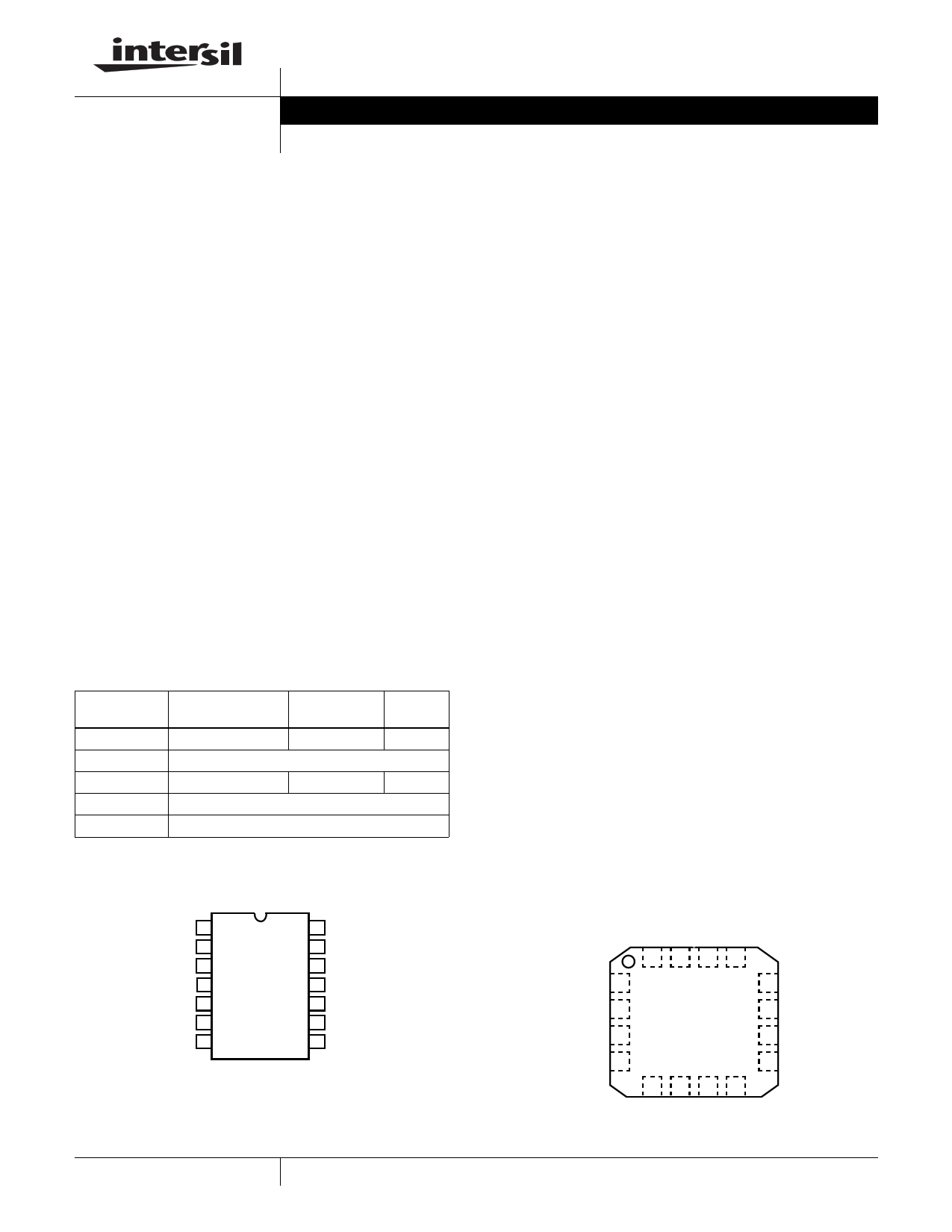
Pinouts
ISL6529 (SOIC)
TOP VIEW
LGATE 1
PGND 2
GND 3
5VCC 4
DRIVE2 5
FB2 6
NC 7
14 UGATE
13 12VCC
12 NC
11 NC
10 COMP
9 FB
8 NC
NC = NO INTERNAL CONNECTION
Features
• Provides two regulated voltages
- One synchronous rectified buck PWM controller
- One linear controller
• Both controllers drive low cost N-Channel MOSFETs
• 12V direct drive saves external components
• Small converter size
- 600kHz constant frequency operation
- Small external component count
• Excellent output voltage regulation
- Both outputs: ±2% over temperature
• 5V down conversion
• PWM and linear output voltage range: down to 0.8V
• Simple single-loop voltage-mode PWM control design
• Fast PWM converter transient response
- High-bandwidth error amplifier
- Full 0–100% duty ratio
• Linear controller drives N-Channel MOSFET pass transistor
• Fully-adjustable outputs
• Undervoltage fault monitoring on both outputs
Applications
• Graphics–GPU and memory supplies
• ASIC power supplies
• Embedded processor and I/O supplies
• DSP supplies
Related Literature
• Technical Brief TB363 Guidelines for Handling and
Processing Moisture Sensitive Surface Mount Devices
(SMDs)
ISL6529 (MLFP)
TOP VIEW
PGND 1
GND 2
5VCC 3
DRIVE2 4
16 15 14 13
12 12VCC
11 NC
10 COMP
9 FB
56 78
NC = NO INTERNAL
CONNECTION
1 CAUTION: These devices are sensitive to electrostatic discharge; follow proper IC Handling Procedures.
1-888-INTERSIL or 321-724-7143 | Intersil (and design) is a trademark of Intersil Americas Inc.
Copyright © Intersil Americas Inc. 2003. All Rights Reserved
All other trademarks mentioned are the property of their respective owners.
1 page 
ISL6529
Electrical Specifications
Recommended Operating Conditions, Unless Otherwise Noted. Refer to Block and Simplified Power System
Diagrams, and Typical Application Schematic (Continued)
PARAMETER
SYMBOL
TEST CONDITIONS
MIN TYP MAX UNITS
UGATE and LGATE Sink Current
UGATE and LGATE OUTPUT IMPEDANCE
LINEAR REGULATOR (DRIVE2)
IGATE
RDS(on)
12VCC = 12V
12VCC = 12V
- 1 -A
- 3.1 4.3 Ω
DC Gain
Gain-Bandwidth Product
Slew Rate
FB2 Input Current
Drive2 High Output Voltage
Drive2 Low Output Voltage
Drive2 High Output Source Current
Drive2 Low Output Sink Current
Over-Voltage Level (VFB2/VREF)
Under-Voltage Level (VFB2/VREF)
REGULATOR ISOLATION
Change in Linear Regulator Output Voltage3
Change in PWM Regulator Output Voltage3
GBWP
SR
II
VOUT High
VOUT Low
IOUT High
IOUT Low
VOV
VUV
∆Vout
∆Vout
RL = 10k, CL = 10pf
RL = 10k, CL = 10pf
RL = 10k, CL = 10pf
VFB2 = 0.8V
Percent of Nominal
Percent of Nominal
Linear Output = 2.5V, 6A Load Change on PWM
PWM Output = 1.5V, 1A Load Change on Linear
-
-
-
-
9.5
-
-0.7
0.85
-
-
-
-
80
15
6
20
10.3
0.1
-1.4
1.2
160
51.5
<0.5
<0.5
- dB
- MHz
- V/µs
150 nA
V
1.0 V
- mA
- mA
-%
-%
-%
-%
NOTE:
3. Measured in the evaluation board.
Functional Pin Descriptions
LGATE 1
PGND 2
GND 3
5VCC 4
DRIVE2 5
FB2 6
NC 7
14 UGATE
13 12VCC
12 NC
11 NC
10 COMP
9 FB
8 NC
NC = NO INTERNAL CONNECTION
LGATE (Pin 1), (Pin 16 MLFP)
Lower gate drive output. Connect to gate of the low-side
MOSFET.
PGND (Pin 2), (Pin 1 MLFP)
This pin is the power ground return for the lower gate driver.
GND (Pin 3), (Pin 2 MLFP)
Signal ground for the IC. All voltage levels are measured with
respect to this pin. Place via close to pin to minimize
impedance path to ground plane.
5VCC (Pin 4), (Pin 3 MLFP)
Provide a well decoupled 5V bias supply for the IC to this
pin. The voltage at this pin is monitored for Power-On Reset
(POR) purposes.
DRIVE2(Pin 5), (Pin 4 MLFP)
Connect this pin to the gate terminal of an external
N-Channel MOSFET transistor. This pin provides the gate
voltage for the linear regulator pass transistor. It also
provides a means of compensating the error amplifier for
applications where the user needs to optimize the regulator
transient response.
FB2 (Pin 6), (Pin 5 MLFP)
Connect the output of the linear regulator to this pin
through a properly sized resistor divider. The voltage at this
pin is regulated to 0.8V. This pin is also monitored for
undervoltage events.
Pulling and holding FB2 above 1.28V shuts down both
regulators. Releasing FB2 initiates soft-start on both regulators.
NC (Pins 7, 8, 11, and 12), (Pins 6, 7, 8, 11, 13 and
15 MLFP)
No internal connection.
FB (Pin 9), (Pin 9 MLFP) and COMP (Pin 10), (Pin
10 MLFP).
FB and COMP are the available external pins of the error
amplifier. The FB pin is the inverting input of the error amplifier
and the COMP pin is the error amplifier output. These pins are
used to compensate the voltage-mode control feedback loop of
the standard synchronous rectified buck converter.
12VCC(Pin 13), (Pin 12 MLFP)
Provides bias voltage for the gate drivers.The voltage at this
pin is monitored for Power-On Reset (POR) purposes.
UGATE (Pin 14), (Pin 14 MLFP)
Connect UGATE to the upper MOSFET gate. This pin
provides the gate drive for the MOSFET.
5
5 Page 
ISL6529
ripple current. The ripple voltage and current are
approximated by the following equations:
∆I
=
V-----I--N-F----–S----V-×----O-L---U----T--
×
-V----O----U----T--
VIN
(EQ. 11)
∆VOUT = ∆I × ESR
(EQ. 12)
Increasing the value of inductance reduces the output ripple
current and voltage ripple. However, increasing the
inductance value will slow the converter response time to a
load transient.
One of the parameters limiting the converter’s response to a
load transient is the time required to slew the inductor
current. Given a sufficiently fast control loop design, the
ISL6529 will provide either 0% or 100% duty cycle in
response to a load transient. The response time is the time
interval required to slew the inductor current from an initial
current value to the final current level. During this interval the
difference between the inductor current and the load current
must be supplied by the output capacitor(s). Minimizing the
response time can minimize the output capacitance
required.
The response time to a transient is different for the
application of load and the removal of load. The following
equations give the approximate response time interval for
application and removal of a transient load:
tRISE
=
-L---O------×-----I--T---R----A----N---
VIN – VOUT
(EQ. 13)
tFALL
=
L----O------×----I--T----R----A----N--
VOUT
(EQ. 14)
where ITRAN is the transient load current step, tRISE is the
response time to the application of load, and tFALL is the
response time to the removal of load.
With a +3.3V input source, the worst case response time can
be either at the application or removal of load and dependent
upon the output voltage setting. Be sure to check both of
these equations at the minimum and maximum output levels
for the worst case response time.
Input Capacitor Selection
The important parameters for the bulk input capacitors are
the voltage rating and the RMS current rating. For reliable
operation, select bulk input capacitors with voltage and
current ratings above the maximum input voltage and largest
RMS current required by the circuit. The capacitor voltage
rating should be at least 1.25 times greater than the
maximum input voltage and a voltage rating of 1.5 times is a
conservative guideline. The RMS current rating requirement
for the input capacitor of a buck regulator is approximately
1/2 of the summation of the DC load current.
Use a mix of input bypass capacitors to control the voltage
overshoot across the switching MOSFETs. Use ceramic
capacitance for the high frequency decoupling and bulk
capacitors to supply the RMS current. Small ceramic
capacitors can be placed very close to the upper MOSFET
to suppress the voltage induced in the parasitic circuit
impedances. Connect them directly to ground with a via
placed very close to the ceramic capacitor footprint.
For a through-hole design, several aluminum electrolytic
capacitors may be needed. For surface mount designs,
tantalum or special polymer capacitors can be used, but
caution must be exercised with regard to the capacitor surge
current rating. These capacitors must be capable of handling
the surge-current at power-up.
TRANSISTOR SELECTION/CONSIDERATIONS
The ISL6529 requires three external transistors. One
N-Channel MOSFET is used as the upper switch in a
standard buck topology PWM converter. Another MOSFET is
used as the lower synchronous switch. The linear controller
drives the gate of an N-Channel MOS transistor used as the
series pass element. The MOSFET transistors should be
selected based upon rDS(ON) , gate supply requirements,
and thermal management considerations.
Upper MOSFET SWITCH Selection
In high-current applications, the MOSFET power dissipation,
package selection and heatsink are the dominant design
factors. The power dissipation includes two loss
components; conduction loss and switching loss. The
conduction losses account for a large portion of the power
dissipation of the upper MOSFET. Switching losses also
contribute to the overall MOSFET power loss.
PCo
n
du
c
t
i
o
nUp
p
er
≅
I
2
o
×
rDS(
on
)
×
D
(EQ. 15)
PSw
itc
h
i
ng
≅
1--
2
Io
×
VI
N
×
tS
W
×
FS
W
(EQ. 16)
where Io is the maximum load current, D is the duty cycle of
the converter (defined as VO/VIN), tSW is the switching
interval, and FSW is the PWM switching frequency.
The lower MOSFET has only conduction loses since it
switches with zero voltage across the device. Conduction
loss is:
PCo
n
du
c
t
i
o
nL
o
w
er
≅
I
2
o
×
rDS(
on
)
×
(
1
–
D
)
(EQ. 17)
These equations assume linear voltage-current transitions
and are approximations. The gate-charge losses are
dissipated by the ISL6529 and do not heat the MOSFET.
However, large gate-charge increases the switching interval,
tSW, which increases the upper MOSFET switching losses.
Ensure that the MOSFET is within its maximum junction
temperature at high ambient temperature by calculating the
11
11 Page | ||
| Páginas | Total 14 Páginas | |
| PDF Descargar | [ Datasheet ISL6529.PDF ] | |
Hoja de datos destacado
| Número de pieza | Descripción | Fabricantes |
| ISL6520 | Single Synchronous Buck Pulse-Width Modulation (PWM) Controller | Intersil Corporation |
| ISL6520A | Single Synchronous Buck Pulse-Width Modulation (PWM) Controller | Intersil Corporation |
| ISL6520B | Single Synchronous Buck Pulse-Width Modulation (PWM) Controller | Intersil Corporation |
| ISL6521 | PWM Buck DC-DC and Triple Linear Power Controller | Intersil |
| Número de pieza | Descripción | Fabricantes |
| SLA6805M | High Voltage 3 phase Motor Driver IC. |
Sanken |
| SDC1742 | 12- and 14-Bit Hybrid Synchro / Resolver-to-Digital Converters. |
Analog Devices |
|
DataSheet.es es una pagina web que funciona como un repositorio de manuales o hoja de datos de muchos de los productos más populares, |
| DataSheet.es | 2020 | Privacy Policy | Contacto | Buscar |