|
|
|
PDF ISL6505 Data sheet ( Hoja de datos )
| Número de pieza | ISL6505 | |
| Descripción | Multiple Linear Power Controller with ACPI Control Interface | |
| Fabricantes | Intersil Corporation | |
| Logotipo | ||
Hay una vista previa y un enlace de descarga de ISL6505 (archivo pdf) en la parte inferior de esta página. Total 17 Páginas | ||
|
No Preview Available !
®
Data Sheet
November 2003
ISL6505
FN9109.1
Multiple Linear Power Controller with
ACPI Control Interface
The ISL6505 complements other power building blocks
(voltage regulators) in ACPI-compliant designs for
microprocessor and computer applications. The IC
integrates three linear controllers/regulators, switching,
monitoring and control functions into a 20-pin wide-body
SOIC or 20-pin QFN (also known as MLF) 5x5 package.
The ISL6505’s operating mode (active or sleep outputs) is
selectable through two digital control pins, S3 and S5.
One linear controller generates the 3.3VDUAL/3.3VSB
voltage plane from the ATX supply’s 5VSB output, powering
the south bridge and the PCI slots through an external NPN
pass transistor during sleep states (S3, S4/S5). In active
state (during S0 and S1/S2), the 3.3VDUAL/3.3VSB linear
regulator uses an external N-channel pass MOSFET to
connect the outputs directly to the 3.3V input supplied by an
ATX power supply, for minimal losses. The
3.3VDUAL/3.3VSB output is active for as long as the ATX 5VSB
voltage is applied to the chip.
A controller powers up the 5VDUAL plane by switching in the
ATX 5V output through an NMOS transistor in active states,
or by switching in the ATX 5VSB through a PMOS (or PNP)
transistor in S3 sleep state. In S4/S5 sleep states, the
ISL6505 5VDUAL output is either shut down or stays on,
based on the state of the EN5 pin.
An internal linear regulator supplies the 1.2V for the voltage
identification circuitry (VID) only during active states (S0 and
S1/S2), and uses the 3V3 pin as input source for its internal
pass element.
A linear controller generates VOUT1 from the
3.3VDUAL/3.3VSB voltage plane, using an external NFET.
The voltage is user-programmable to values between 1.2V
and 1.5V, using an external resistor divider. The mode is
user-selectable with the LAN pin; a logic high (or open)
selects the 10/100 LAN mode, where VOUT1 is always on
(S0-S5); a logic low selects the Gigabit Ethernet mode,
where VOUT1 is only on during active modes (S0-S2).
Ordering Information
Features
• Provides four ACPI-Controlled Voltages
- 5VDUAL USB/Keyboard/Mouse
- 3.3VDUAL/3.3VSB PCI/Auxiliary/LAN
- 1.2VVID Processor VID Circuitry
- VOUT1 (1.2V - 1.5V programmable) LAN/Ethernet
• Excellent Output Voltage Regulation
- All Outputs: ±2.0% over temperature (as applicable)
• Small Size; Very Low External Component Count
• Undervoltage Monitoring of All Outputs with Centralized
FAULT Reporting and Temperature Shutdown
• QFN Package:
- Compliant to JEDEC PUB95 MO-220
QFN - Quad Flat No Leads - Package Outline
- Near Chip Scale Package footprint, which improves
PCB efficiency and has a thinner profile
Applications
• ACPI-Compliant Power Regulation for Motherboards
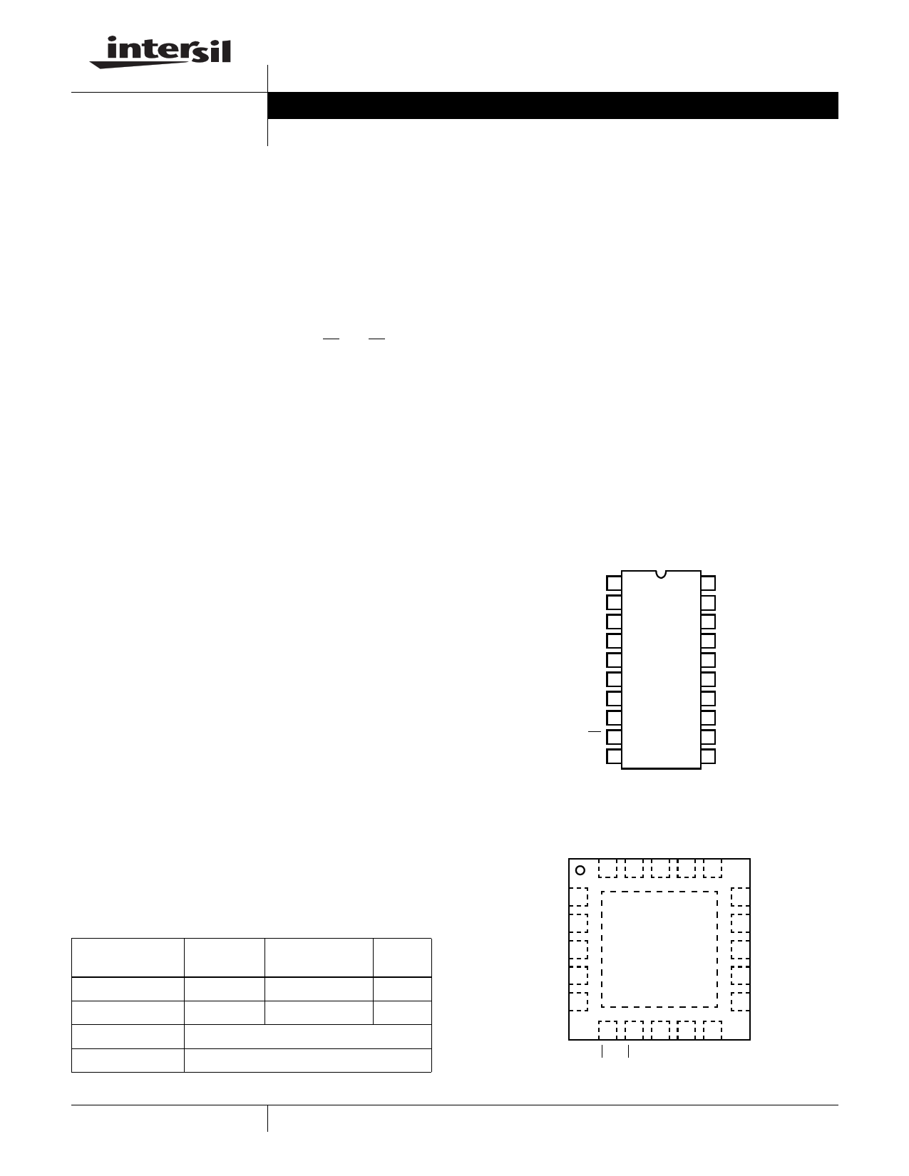
Pinouts
ISL6505 (20-LEAD-WIDE SOIC) TOP VIEW
FB1 1
DR1 2
3V3DLSB 3
3V3DL 4
1V2VID 5
3V3 6
5V 7
EN5 8
S3 9
S5 10
20 5VSB
19 VID_CT
18 VID_PG
17 SS
16 LAN
15 5VDL
14 5VDLSB
13 DLA
12 FAULT
11 GND
ISL6505 (5 X 5 QFN) TOP VIEW
20 19 18 17 16
3V3DL 1
1V2VID 2
15 VID_PG
14 SS
TEMP.
PART NUMBER RANGE (oC)
PACKAGE
PKG.
DWG. #
ISL6505CB
0 to 70 20 Ld Wide SOIC M20.3
ISL6505CR
0 to 70 20 Ld 5x5 QFN L20.5x5
ISL6505EVAL1
Evaluation Board (SOIC)
ISL6505AEVAL2 Evaluation Board (QFN)
3V3 3
5V 4
EN5 5
13 LAN
12 5VDL
11 5VDLSB
6 7 8 9 10
NOTE: The QFN bottom pad is electrically connected to the IC substrate, at GND potential.
It can be left unconnected, or connected to GND; do NOT connect to another potential.
1 CAUTION: These devices are sensitive to electrostatic discharge; follow proper IC Handling Procedures.
1-888-INTERSIL or 321-724-7143 | Intersil (and design) is a registered trademark of Intersil Americas Inc.
Copyright © Intersil Americas Inc. 2003. All Rights Reserved
All other trademarks mentioned are the property of their respective owners.
1 page 
ISL6505
Electrical Specifications Recommended Operating Conditions, Unless Otherwise Noted Refer to Figures 1, 2 and 3 (Continued)
PARAMETER
SYMBOL
TEST CONDITIONS
MIN TYP MAX UNITS
1.2VVID LINEAR REGULATOR (VOUT2)
1V2VID Regulation
- - 2.0 %
1V2VID Nominal Voltage Level
1V2VID Undervoltage Rising Threshold
V1V2VID
- 1.2 -
- 0.92 -
V
V
1V2VID Undervoltage Hysteresis
- 100 -
mV
1V2VID Output Current
I1V2VID
3.3VDUAL/3.3VSB LINEAR REGULATOR (VOUT3)
3V3DL Sleep State Regulation
V3V3 = 3.3V
- - 180 mA
- - 2.0 %
3V3DL Nominal Voltage Level
3V3DL Undervoltage Rising Threshold
V3V3DL
- 3.3 -
- 2.62 -
V
V
3V3DL Undervoltage Hysteresis
- 150 -
mV
3V3DLSB Output Drive Current
5VDUAL SWITCH CONTROLLER (VOUT4)
5VDL Undervoltage Rising Threshold
I3V3DLSB V5VSB = 5V
30 50
-
mA
- 4.10 -
V
5VDL Undervoltage Hysteresis
- 120 -
mV
5VDLSB Output Drive Current
TIMING INTERVALS
I5VDLSB V5VDLSB = 4V, V5VSB = 5V
-20 - -40 mA
Active State Assessment Past Input UV
Thresholds (Note 4)
42 53 64
ms
Active-to-Sleep Control Input Delay
- 200 -
µs
Falling UV Threshold Timeout (All Monitors)
CONTROL I/O (S3, S5, EN5, LAN, FAULT)
- 10 -
µs
High Level Input Threshold
S3, S5, EN5, LAN
- - 2.2 V
Low Level Input Threshold
S3, S5, EN5, LAN
0.8 -
-
V
Internal Pull-up Current to 5VSB
S3, S5 to GND
- 50 -
µA
Internal Pull-up Current to 5VSB
EN5, LAN to GND
- 10 -
µA
Input Leakage Current to 5VSB
EN5, LAN to 5VSB
- - 10 µA
FAULT Current Ioh (to 5VSB)
FAULT = 4.6V, 5VSB = 5V
- -7.5 -
mA
FAULT Current Iol (to GND)
TEMPERATURE MONITOR
Fault-Level Threshold (Note 5)
Shutdown-Level Threshold (Note 5)
NOTES:
4. Guaranteed by Correlation.
5. Guaranteed by Design.
FAULT = 0.4V, 5VSB = 5V
- 0.75 -
125 -
- 155
-
-
mA
oC
oC
5
5 Page 
ISL6505
80
70
60
50
40
30
20
10
0
01 2 3 4 5 6 7
VID_PG DELAY (ms)
FIGURE 10. VID_PG DELAY DEPENDENCE
ON VID_CT CAPACITOR
8
9 10
The value of the VID_CT capacitor to be used to obtain a
given VID_PG delay can be determined from the graph in
Figure 10. For extended delays exceeding the range of the
graph, use the following formula:
C
=
-t-D-----E----L---A----Y--
125000
, where
tDELAY - desired delay time (s)
C - VID_CT capacitor to obtain desired delay time (F)
If no delay is needed, then a very small (pF) capacitor, or
even no capacitor at all will generate a very short delay (just
the pin capacitance of ~10pF should give a delay of ~1µs).
The value of the external VID_PG pull-up resistor is
determined by the trade-off between the pull-down current
available from the pin versus the rise time needed. In the
typical power-up sequence (as described above), the
VID_PG starts low (VID Power NOT Good) until the 1V2VID
output reaches its power-good threshold (90%), which starts
the VID_CT pin charging. When that pin reaches its trip
point, the VID_PG pin open-drain pull-down device shuts off,
and the external pull-up resistor (R2, as shown in Figure 13)
will pull the output up to the positive supply (typically
1V2VID). This rise time is determined not by the ISL6505,
but simply by the RC time constant of the pull-up resistor,
and whatever capacitance is on the node, from the VID_PG
output pin to whatever signals it is driving, including the pin
capacitances and all of the parasitics; this may vary from
one system implementation to another.
The R2 value in Figure 13 (and on the ISL6505EVAL1/2
boards) is listed as 10kΩ, which may work fine in some
systems. However, some of the newer systems may require
a faster rise time than allowed by the 10kΩ resistor, so a
lower value of resistance should be chosen. But the VID_PG
pin must be able to pull down low enough against the
resistor to guarantee a low logic level for whatever control
signals it is driving. Since the pin can nominally sink 1.2mA
with only a 0.1V drop, a 1kΩ resistor will match that
condition. The minimum input low logic level is typically
around 25-30% of the 1.2V supply (0.3V in this example),
and the 0.1V is well below it. So a resistor pull-up value as
low as 1kΩ is acceptable to get faster rise times.
Linear Regulator (VOUT1) Compensation
VOUT1 is a linear regulator, with an on-chip amplifier, and
external FET and feedback resistors. The output capacitors
should be selected to allow the output voltage to meet any
dynamic regulation requirements, paying attention to their
parasitic components ESR (Effective Series Resistance) and
ESL (Effective Series inductance).
VOUT1 is internally compensated to cover a wide range of
load currents; however the output filter capacitor must be
chosen carefully. Ideally, the capacitor value and its ESR
combine to create a zero that cancels one of the amplifier
poles. However, this is only a first order approximation, since
that pole moves with load current, for example. In addition,
there are high frequency poles that may come into play
under certain conditions.
A lower capacitor ESR improves transient response. When
the output load changes quickly (faster than the amplifier
itself can respond), the differential load current is sourced or
sinked by the capacitor, until the regulator can respond and
catch up. In this case, the higher the ESR, the larger the
voltage drop across it, and thus the larger the voltage
transient on the output is.
However, lower output capacitor ESR pushes the zero
frequency higher, reducing the regulator phase margin.
Thus, it may be difficult to simultaneously satisfy both tight
dynamic regulation and a good stable loop with high phase
margin.
There are many factors that affect VOUT1 stability, such that
a simple equation or formula is not practical. So the
recommendation is to choose a value from Figure 11, which
shows capacitance versus ESR. Values inside the polygon
will result in stable conditions over a full load range of 10mA
to 3A. Choosing a value outside the polygon is NOT
recommended; it may work in some cases, but the margin
may be much smaller. In addition, there are manufacturing
tolerances (of both the IC and the capacitor), load variations,
temperature, FET selection, and many other factors that can
create the potential for problems.
ESR vs CAPACITANCE
1000
100
10
100
1000
CAPACITANCE (uF)
10000
FIGURE 11. VOUT1 OUTPUT CAPACITOR SELECTION
11
11 Page | ||
| Páginas | Total 17 Páginas | |
| PDF Descargar | [ Datasheet ISL6505.PDF ] | |
Hoja de datos destacado
| Número de pieza | Descripción | Fabricantes |
| ISL6504 | Multiple Linear Power Controller with ACPI Control Interface | Intersil Corporation |
| ISL6504A | Multiple Linear Power Controller with ACPI Control Interface | Intersil Corporation |
| ISL6505 | Multiple Linear Power Controller with ACPI Control Interface | Intersil Corporation |
| ISL6505AEVAL2 | Multiple Linear Power Controller with ACPI Control Interface | Intersil Corporation |
| Número de pieza | Descripción | Fabricantes |
| SLA6805M | High Voltage 3 phase Motor Driver IC. |
Sanken |
| SDC1742 | 12- and 14-Bit Hybrid Synchro / Resolver-to-Digital Converters. |
Analog Devices |
|
DataSheet.es es una pagina web que funciona como un repositorio de manuales o hoja de datos de muchos de los productos más populares, |
| DataSheet.es | 2020 | Privacy Policy | Contacto | Buscar |