|
|
|
PDF ISL56403IN Data sheet ( Hoja de datos )
| Número de pieza | ISL56403IN | |
| Descripción | 3V Dual 8-Bit/ 20/40/60MSPS A/D Converter with Internal Voltage Reference | |
| Fabricantes | Intersil Corporation | |
| Logotipo | ||
Hay una vista previa y un enlace de descarga de ISL56403IN (archivo pdf) en la parte inferior de esta página. Total 11 Páginas | ||
|
No Preview Available !
ADVANCE INFORMATION Data Sheet
ISL5640
June 2000 File Number 4657.3
3V Dual 8-Bit, 20/40/60MSPS A/D
Converter with Internal Voltage Reference
The ISL5640 is a monolithic, dual 8-bit analog-to-digital
converter fabricated in an advanced CMOS process. It is
designed for high speed applications where integration,
bandwidth and accuracy are essential. The ISL5640
features a 9-stage pipeline architecture. The fully pipelined
architecture and an innovative input stage enable the
ISL5640 to accept a variety of input configurations, single-
ended or fully differential. Only one external clock is
necessary to drive both converters and an internal band-gap
voltage reference is provided. This allows the system
designer to realize an increased level of system integration
resulting in decreased cost and power dissipation.
The ISL5640 has excellent dynamic performance while
consuming less than 100mW power at 40MSPS. The A/D
only requires a single +3.0V power supply. Data output
latches are provided which present valid data to the output
bus with a latency of 5 clock cycles.
The ISL5640 is offered in 20MSPS, 30MSPS, 40MSPS and
60MSPS sampling rates.
Ordering Information
PART
NUMBER
ISL5640/2IN
TEMP.
RANGE
(oC)
PACKAGE
SAMPLING
RATE
PKG. NO. (MSPS)
-40 to 85 48 Ld LQFP Q48.7x7
20
ISL5640/3IN -40 to 85 48 Ld LQFP Q48.7x7
ISL5640/4IN -40 to 85 48 Ld LQFP Q48.7x7
ISL5640/6IN -40 to 85 48 Ld LQFP Q48.7x7
ISL5640 EVAL 25 Evaluation Platform
30
40
60
Features
• Sampling Rate . . . . . . . . . . . . . . . . . . . . . . . . . . .40MSPS
• 7.4 Bits at fIN = 1MHz
• Low Power at 40MSPS. . . . . . . . . . . . . . . . . . . . . 100mW
• Power Down Mode . . . . . . . . . . . . . . . . . . . . . . . . . <1mW
• Wide Full Power Input Bandwidth. . . . . . . . . . . . . 250MHz
• SFDR at fIN = 1MHz . . . . . . . . . . . . . . . . . . . . . . . . . .55dB
• Excellent Channel-to-Channel Isolation . . . . . . . . . >75dB
• On-Chip Sample and Hold Amplifiers
• Internal Bandgap Voltage Reference . . . . . . . . . . . . 1.25V
• Single Supply Voltage Operation . . . . . . . . . . . . . . . +3.0V
• Offset Binary or Two’s Complement Output Format
• Dual 8-Bit A/D Converters on a Monolithic Chip
• Pin Compatible Upgrade to AD9288
Applications
• Wireless Local Loop
• PSK and QAM I&Q Demodulators
• Medical Imaging
• High Speed Data Acquisition
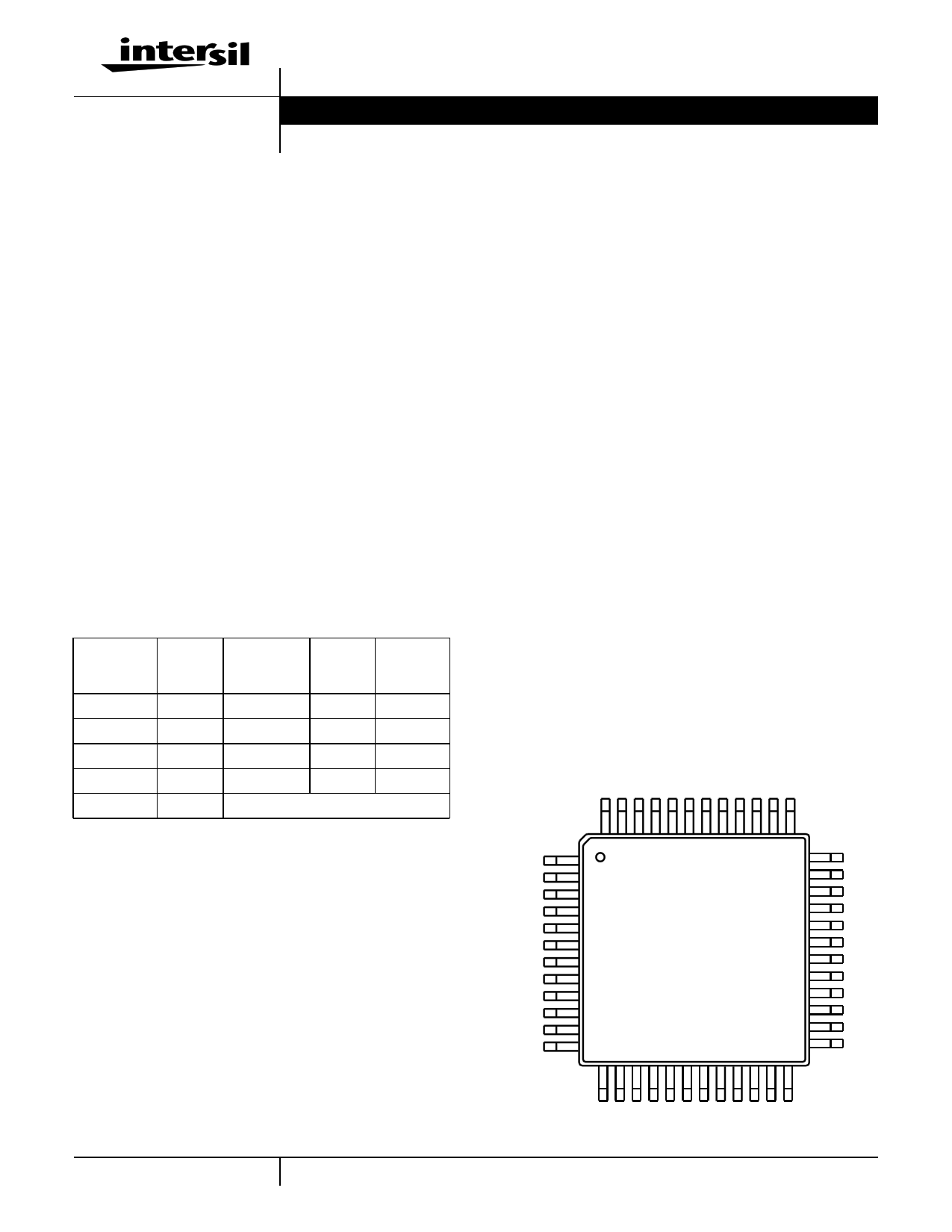
Pinout
48 LEAD LQFP
TOP VIEW
GND
IIN+
IIN-
DFS
IVRIN
VROUT
QVRIN
S1
S2
QIN-
QIN+
GND
48 47 46 45 44 43 42 41 40 39 38 37
1 36
2 35
3 34
4 33
5 32
6 31
7 30
8 29
9 28
10 27
11 26
12 25
13 14 15 16 17 18 19 20 21 22 23 24
N/C
N/C
GND
DVCC
GND
AVCC
AVCC
GND
DVCC
GND
N/C
N/C
3-1 CAUTION: These devices are sensitive to electrostatic discharge; follow proper IC Handling Procedures.
1-888-INTERSIL or 321-724-7143 | Copyright © Intersil Corporation 2000
1 page 
ISL5640
Absolute Maximum Ratings TA = 25oC
Supply Voltage, AVCC or DVCC to AGND or DGND . . . . . . . . . . .4V
DGND to AGND . . . . . . . . . . . . . . . . . . . . . . . . . . . . . . . . . . . . . . . . 0.3V
Digital I/O Pins . . . . . . . . . . . . . . . . . . . . . . . . . . . . . DGND to DVCC
Analog I/O Pins . . . . . . . . . . . . . . . . . . . . . . . . . . . . AGND to AVCC
Operating Conditions
Thermal Information
Thermal Resistance (Typical, Note 1)
θJA (oC/W)
ISL5640IN . . . . . . . . . . . . . . . . . . . . . . . . . . . . . . . .
70
Maximum Junction Temperature . . . . . . . . . . . . . . . . . . . . . . .150oC
Maximum Storage Temperature Range . . . . . . . . . . -65oC to 150oC
Maximum Lead Temperature (Soldering 10s) . . . . . . . . . . . . .300oC
(Lead Tips Only)
Temperature Range
ISL5640IN . . . . . . . . . . . . . . . . . . . . . . . . . . . . . . . -40oC to 85oC
CAUTION: Stresses above those listed in “Absolute Maximum Ratings” may cause permanent damage to the device. This is a stress only rating and operation of the
device at these or any other conditions above those indicated in the operational sections of this specification is not implied.
Electrical Specifications
AVDD = DVDD
CL = 10pF; TA
=
=
2+53o.3CV; ;UVnIlNes=s1O.5th0eVr;wfSise=
40MSPS
Specified
at
50%
Duty
Cycle;
PARAMETER
TEST CONDITIONS
MIN
ACCURACY
Resolution
8
Integral Linearity Error, INL
Differential Linearity Error, DNL
(Guaranteed No Missing Codes)
fIN = 1MHz
fIN = 1MHz
-
-
Offset Error, VOS
Full Scale Error, FSE
DYNAMIC CHARACTERISTICS
fIN = DC
fIN = DC
-10
-
Minimum Conversion Rate
No Missing Codes
-
Maximum Conversion Rate
No Missing Codes
40
Effective Number of Bits, ENOB
Signal to Noise and Distortion Ratio, SINAD
= R-----M-----S------NR----oM---i--sS---e---S--+--i-g--D--n--i-as---lt--o---r--t--i-o----n-
fIN = 1MHz
fIN = 1MHz
-
-
Signal to Noise Ratio, SNR
= R-R----M-M----S-S-----SN----i-og---in-s---ae---l
fIN = 10MHz
-
TYP
-
0.5
±0.2
-
1
-
-
7.5
46
47
MAX
-
-
±1.0
+10
-
-
-
-
-
-
UNITS
Bits
LSB
LSB
LSB
LSB
MSPS
MSPS
Bits
dB
dB
Total Harmonic Distortion, THD
2nd Harmonic Distortion
3rd Harmonic Distortion
Spurious Free Dynamic Range, SFDR
Intermodulation Distortion, IMD
I/Q Channel Crosstalk
I/Q Channel Offset Match
I/Q Channel Full Scale Error Match
Transient Response
Over-Voltage Recovery
ANALOG INPUT
Maximum Peak-to-Peak Single-Ended
Analog Input Range
Analog Input Resistance, RINA or RINB
Analog Input Capacitance, CINA or CINB
fIN = 10MHz
fIN = 10MHz
fIN = 10MHz
fIN = 10MHz
f1 = 1MHz, f2 = 1.02MHz
(Note 2)
0.2V Overdrive (Note 2)
VINA, VINB = VREF, DC
VINA, VINB = 1.5V, DC
- -53 -
dBc
- -54 -
dBc
- -70 -
dBc
- 54 - dBc
- - - dBc
- - - dBc
- - - LSB
- - - LSB
- - - Cycle
- - - Cycle
- 1.0 -
---
---
V
MΩ
pF
3-5
5 Page 
ISL5640
All Intersil semiconductor products are manufactured, assembled and tested under ISO9000 quality systems certification.
Intersil semiconductor products are sold by description only. Intersil Corporation reserves the right to make changes in circuit design and/or specifications at any time with-
out notice. Accordingly, the reader is cautioned to verify that data sheets are current before placing orders. Information furnished by Intersil is believed to be accurate and
reliable. However, no responsibility is assumed by Intersil or its subsidiaries for its use; nor for any infringements of patents or other rights of third parties which may result
from its use. No license is granted by implication or otherwise under any patent or patent rights of Intersil or its subsidiaries.
For information regarding Intersil Corporation and its products, see web site www.intersil.com
Sales Office Headquarters
NORTH AMERICA
Intersil Corporation
P. O. Box 883, Mail Stop 53-204
Melbourne, FL 32902
TEL: (321) 724-7000
FAX: (321) 724-7240
EUROPE
Intersil SA
Mercure Center
100, Rue de la Fusee
1130 Brussels, Belgium
TEL: (32) 2.724.2111
FAX: (32) 2.724.22.05
ASIA
Intersil Ltd.
8F-2, 96, Sec. 1, Chien-kuo North,
Taipei, Taiwan 104
Republic of China
TEL: 886-2-2515-8508
FAX: 886-2-2515-8369
3-11
11 Page | ||
| Páginas | Total 11 Páginas | |
| PDF Descargar | [ Datasheet ISL56403IN.PDF ] | |
Hoja de datos destacado
| Número de pieza | Descripción | Fabricantes |
| ISL56403IN | 3V Dual 8-Bit/ 20/40/60MSPS A/D Converter with Internal Voltage Reference | Intersil Corporation |
| Número de pieza | Descripción | Fabricantes |
| SLA6805M | High Voltage 3 phase Motor Driver IC. |
Sanken |
| SDC1742 | 12- and 14-Bit Hybrid Synchro / Resolver-to-Digital Converters. |
Analog Devices |
|
DataSheet.es es una pagina web que funciona como un repositorio de manuales o hoja de datos de muchos de los productos más populares, |
| DataSheet.es | 2020 | Privacy Policy | Contacto | Buscar |