|
|
|
PDF ISL5239 Data sheet ( Hoja de datos )
| Número de pieza | ISL5239 | |
| Descripción | Pre-Distortion Linearizer | |
| Fabricantes | Intersil Corporation | |
| Logotipo | ||
Hay una vista previa y un enlace de descarga de ISL5239 (archivo pdf) en la parte inferior de esta página. Total 30 Páginas | ||
|
No Preview Available !
®
Data Sheet
July 2002
ISL5239
FN8039.1
Pre-Distortion Linearizer
The ISL5239 Pre-Distortion Linearizer
(PDL) is a full featured component for
Power Amplifier (PA) linearization to
improve PA power efficiency and reduce PA cost.
The Radio Frequency (RF) PA is one of the most expensive and
power-consuming devices in any wireless communication
system. The ideal RF PA would have an entirely linear
relationship between input and output, expressed as a simple
gain which applies at all power levels. Unfortunately, realizable
RF amplifiers are not completely linear and the use of pre-
distortion techniques allows the substitution of lower cost/power
PA’s for higher cost/power PA’s.
The ISL5239 pre-distortion linearizer enables the linearization of
less expensive PA’s to provide more efficient operation closer to
saturation. This provides the benefit of improved linearity and
efficiency, while reducing PA cost and operational expense.
The ISL5239 features a 125MHz pre-distortion bandwidth
capable of full 5th order intermodulation correction for signal
bandwidths up to 20MHz. This bandwidth is particularly well
suited for 3G cellular deployments of UMTS and CDMA2000.
The device also corrects for PA memory effects that limit pre-
distortion performance including self heating.
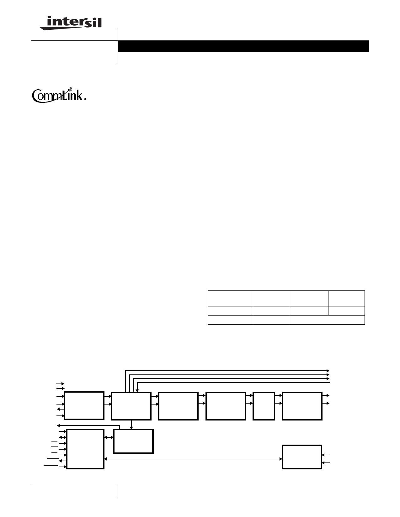
The ISL5239 combines an input formatter and interpolator, pre-
distortion linearizer, an IF converter, correction filter,
gain/phase/offset adjustment, output formatter, and input and
feedback capture memories into a single chip controlled by a 16-
bit linearizer interface.
The ISL5239 supports log of power, linear magnitude, and linear
power based pre-distortion, utilizing two Look-Up Table (LUT)
based algorithms for the pre-distortion correction. The device
provides programmable scaling and offset correction, and
provides for phase imbalance adjustment.
Block Diagram
Features
• Output Sample Rates Up to 125MSPS
• Full 20MHz Signal Bandwidth
• Dynamic Memory Effects Compensation
• Input and Feedback Capture Memories
• LUT-based Digital Pre-distortion
• Two 18-bit Output Busses with Programmable Bit-Width
• 16-Bit Parallel µProcessor Interface
• Input Interpolator x2, x4, x8
• Programmable Frequency Response Correction
• Low Power Architecture
• Threshold Comparator for Internal Triggering
• Quadrature or Digital IF Architecture
• Lowest-Cost Full-Featured Part Available
Applications
• Base Station Power Amplifier Linearization
• Operates with ISL5217 in Software Radio Solutions
• Compatible with the ISL5961 or ISL5929 D/A Converters
Ordering Information
PART
NUMBER
ISL5239KI
ISL5239EVAL1
TEMP
RANGE (oC) PACKAGE
-40 to 85 196 Ld BGA
25 Evaluation Kit
PKG. DWG. #
V196.15x15
CLK
TRIGIN
IIN<17:0>
QIN<17:0>
CLKOUT
ISTRB
TRIGOUT
A<5:0>
P<15:0>
CS
WR
RD
BUSY
RESET
INPUT
FORMATTER
AND
INTERPOLATOR
X1, X2, X4, X8
uP INTERFACE
PRE-DISTORTER
WITH
TWO 1K x 60
LUTs
INPUT
MEMORY
(2k x 32)
IF CONVERTER
REAL 1X
REAL 2X
COMPLEX
CORRECTION
FILTER
REAL 1X
REAL 2X
COMPLEX
GAIN /
PHASE
OFFSET
ADJUST
OUTPUT
DATA
FORMATTER
8-18 BIT-WIDTH
SERCLK
SERSYNC
SEROUT
SERIN
IOUT<17:0>
QOUT<17:0>
FEEDBACK
MEMORY
(1k x 20)
FBCLK
FB<19:0>
1 CAUTION: These devices are sensitive to electrostatic discharge; follow proper IC Handling Procedures.
1-888-INTERSIL or 321-724-7143 | Intersil (and design) is a registered trademark of Intersil Americas Inc.
Copyright © Intersil Americas Inc. 2002. All Rights Reserved
CommLink™ is a trademark of Intersil Americas Inc.
1 page 
ISL5239
Functional Description
The ISL5239 is a full-featured digital pre-distortion part
featuring a high-performance lookup-table based pre-
distortion (PD) processing unit. It includes an interpolator for
upsampling and supports all varieties of upconversion
architectures with a programmable correction filter for
equalization including both sin(x)/x correction and removal of
frequency response imbalance between quadrature paths. It
also features gain, phase, and offset compensation for direct
upconversion, digital IF output for heterodyning, and
input/output capture memories with internal/external
triggering capabilities to facilitate closedloop feedback
processing. System implementation is typically as shown in
Figure 1. Although the power detect feedback is shown with
one Analog to Digital Converter (ADC), coherently
demodulated feedback signalsLO configurations with 1 or 2
ADC’s are also supported.
The block diagram on page 1 shows the internal functional
units within the ISL5239. In the following sections each
functional unit is described. The operation of the ISL5239 is
controlled by the register map listed in Table 3. Detailed
descriptions for each control/status register are given in
Tables 4 through 48. The control/status registers are
referred to in the discussion below.
FIGURE 1. SYSTEM OVERVIEW
Input Formatter and Interpolator (IFIP)
The Input Formatter and Interpolator interfaces to the data
source to provide for parallel data input via the IIN<17:0>,
QIN<17:0> busses, or serial input via the IIN<17:0> input
bus. In parallel input mode, both 18-bit input busses are
used to allow for parallel I and Q sample loading. In serial
mode, the data is input via the IIN<17:0> bus only, as the I
sample followed by the Q sample with the ISTRB input
asserted with each I sample. In this mode, the QIN<17:0>
bus is not utilized. The input data format is selectable as
either two’s complement or offset binary.
The Interpolator function is necessary because pre-distorting
a signal results in a much wider bandwidth signal (typically
5x to 7x wider). The Input Formatter and Interpolator is
depicted in Figure 2.
Three interpolation rates (x2, x4, and x8) are supported by
the cascade of three Half-Band (HB) Filters. The ISL5239
includes an on-chip clock divider to facilitate input clocking.
The clock divider generates the CLKOUT signal which is
used to clock data from the input signal source. Typical input
sources include the ISL5217 quad programmable
upconverter, which is designed to operate seamlessly with
the ISL5239.
The interpolation factor is selectable in control word 0x02,
bits 6:4 as x1, x2, x4, and x8. The x1 mode bypasses all
three half-band filters. The x2 mode utilized HB1 and
bypasses HB2 and HB3. The x4 mode utilized HB1 and HB2
and bypasses HB3. Finally, the x8 mode utilizes all three
HBFs. Saturation status bits are provided for each of the
three HBFs in the status register 0x03.
Input data rates up to the CLK rate are supported, based on
the requirement CLK >= Fs * IP, where Fs is the input rate of
the incoming data and IP is the interpolation factor selected
in control word 0x02.
IIN<17:0>
QIN<17:0>
BYPASS BYPASS BYPASS
HALF
BAND
HALF
BAND
HALF
BAND
I
/
18
FILTER
1
/
20
FILTER
2
/
20
FILTER
3
2/0
Q
FIGURE 2. INPUT FORMATTER AND INTERPOLATOR
BLOCK DIAGRAM
Each half-band filter performs a x2 interpolation by inserting
one zero between each input data sample, causing the
sampling frequency to double. The resulting zero-stuffed
data is then low pass filtered to reject the upsampling image.
The half-band filter frequency responses are as shown in
Figure 3.
HALFBAND FILTER 1 RESPONSE
0
-20
-40
-60
-80
-100
-120
-140
0
0.1 0.2 0.3 0.4 0.5 0.6 0.7 0.8 0.9
NORMALIZED FREQUENCY (NYQUIST=1)
1
FIGURE 3. x2, HB1 ENABLED FREQUENCY RESPONSE
5
5 Page 
ISL5239
General Comments About Modes
Once a trigger is detected in the ARMED condition, all
following triggers are ignored during the sequence. The
system does not acknowledge new triggers until a new
transaction is invoked and re-armed. When a new mode is
invoked, all subsequent invocations of new modes during
the duration of its sequence is ignored, except in the loop
mode. In the loop mode, an input memory mode change to
IDLE is processed immediately.
When in the IDLE, all controls, addresses, and data, default
to the processor interface values.
Triggers
When a capture memory is ARMED, i.e. waiting for a trigger
to happen, the activation of the trigger occurs in three ways
— external, data dependent, and user invoked. The trigger
select, 0x04, bits 5:4, provides the selection of the trigger
source. When the pre-distorter magnitude bus values fall
between the range of 0x09 minimum and 0x0a maximum,
the data dependent trigger activates. The first of these
transitions causes a trigger to be detected and the remaining
triggers during the capture sequence is ignored.
To invoke the user invoked trigger, 0x04, 5:4, set to
processor, the programmer writes a TRIGGER to the 0x04,
bit 6 processor trigger register. After a TRIGGER is in the
field, the user initiates the trigger by just writing to that
register. The user does not have to reset the trigger back to
IDLE. By setting the processor trigger bit to IDLE when not in
use, it keeps the circuit quiet and allows the user to write to
other values at that address without causing a trigger to
occur during operation. To disable the processor trigger, the
user should change trigger select to something other than
PROCESSOR and then change values in processor trigger.
If trigger select is not set to PROCESSOR, the system
ignores the trigger generated by processor trigger.
The feedback and input memory circuit uses the same
trigger; both circuits trigger at the same point with its
operation registers causing different operations to occur.
The user should monitor input memory status and feedback
memory status simultaneously before activating triggers.
Make sure both status registers are in ARMED before
activating triggers or the results from the capture can be
erroneous and data can be overwritten. Selecting processor
trigger (register 0x04, bits 5:4 = 00) while arming the input
and feedback memory circuits is a convenient way to ensure
no unexpected triggers occur before confirming ARMED
status of both circuits.
Input Data to Input Memory
There are three sources of input data to the input memory —
interpolator, pre-distorter’s data outputs, and the pre-
distorter’s magnitude. Data from the interpolator and the
predistort output are the upper 16 bits with or without
rounding. Only 16 of the original 20 bits of I or Q is loaded
into the memory. The I data is read from the memory on the
DataHigh register and the Q data, DataLow register.
In the predistort magnitude input, the data is unsigned 16
bits and the software has to reshuffle the data to extract the
original magnitude. The DataHigh contains only the pre-
distorter magnitude bit 15, and the DataLow contains the
pre-distorter magnitude 14:0.
Writing/Reading the Memories from the Processor
Interface
In the auto-increment mode, the data is loaded in 16-bit
increments. The low word is written or read first followed by
the high word. The high word increments the address
counter and generates the actual write to the memory. For
reading, it just increments the counter. The input memory
select 0x04, bit 12, selects the memory to be written to or
read from.
When writing or reading a specific address, the 0x0b
address register must be loaded before the 0x0c and 0x0d
memory data registers. In the write, the high word
transaction will trigger the actual write to the memory and a
low word must be written first. For additional details, see the
uP interface section.
Microprocessor Interface
The microprocessor interface allows the ISL5239 to appear
as a memory mapped peripheral to the µP. All registers can
be accessed through this interface. The interface consists of
a 16 bit bidirectional data bus, P<15:0>, six bit address bus,
A<5:0>, a write strobe (WR), a read strobe (RD) and a chip
enable (CE). The interface is configured for separate read
and write strobe inputs.
The processor interface provides a simple parallel
Data/Control/Address bus for monitoring and controlling its
operation. The processor interface is asynchronous to the
CLK, and BUSY signal is included to indicate when read and
write operations are complete.
The register configuration is master/slave, where the slave
registers are updated from the masters and all reads access
the slaves.
The master registers are clocked by the µP WR strobe, are
writable and cleared by a hard reset. The slave registers are
clocked by CLK, and are readable and cleared by either a
hard or soft reset. The transfer of configuration data from the
master register to the slave register occurs synchronously
after an event and requires a four clock synchronization
period.
The µP can perform back-to-back accesses to the register,
but must maintain four fCLK periods between accesses to
the same address. This limits the maximum µP access rate
for the RAM to 125MHz/4 = 31.25MHz.
11
11 Page | ||
| Páginas | Total 30 Páginas | |
| PDF Descargar | [ Datasheet ISL5239.PDF ] | |
Hoja de datos destacado
| Número de pieza | Descripción | Fabricantes |
| ISL5239 | Pre-Distortion Linearizer | Intersil Corporation |
| ISL5239EVAL1 | Pre-Distortion Linearizer | Intersil Corporation |
| ISL5239KI | Pre-Distortion Linearizer | Intersil Corporation |
| Número de pieza | Descripción | Fabricantes |
| SLA6805M | High Voltage 3 phase Motor Driver IC. |
Sanken |
| SDC1742 | 12- and 14-Bit Hybrid Synchro / Resolver-to-Digital Converters. |
Analog Devices |
|
DataSheet.es es una pagina web que funciona como un repositorio de manuales o hoja de datos de muchos de los productos más populares, |
| DataSheet.es | 2020 | Privacy Policy | Contacto | Buscar |