|
|
|
PDF IS89C52-24PQI Data sheet ( Hoja de datos )
| Número de pieza | IS89C52-24PQI | |
| Descripción | CMOS SINGLE CHIP 8-BIT MICROCONTROLLER with 8-Kbytes of FLASH | |
| Fabricantes | Integrated Silicon Solution Inc | |
| Logotipo | ||
Hay una vista previa y un enlace de descarga de IS89C52-24PQI (archivo pdf) en la parte inferior de esta página. Total 50 Páginas | ||
|
No Preview Available !
IISS898C952C52
CMOS SINGLE CHIP
8-BIT MICROCONTROLLER
with 8-Kbytes of FLASH
ISSIISSI®®
NOVEMBER 1998
FEATURES
• 80C51 based architecture
• 8-Kbytes of on-chip Reprogrammable Flash
Memory
• 256 x 8 RAM
• Three 16-bit Timer/Counters
• Full duplex serial channel
• Boolean processor
• Four 8-bit I/O ports, 32 I/O lines
• Memory addressing capability
– 64K ROM and 64K RAM
• Program memory lock
– Lock bits (3)
• Power save modes:
– Idle and power-down
• Eight interrupt sources
• Most instructions execute in 0.3 µs
• CMOS and TTL compatible
• Maximum speed: 40 MHz @ Vcc = 5V
• Industrial temperature available
• Packages available:
– 40-pin DIP
– 44-pin PLCC
– 44-pin PQFP
GENERAL DESCRIPTION
The ISSI IS89C52 is a high-performance microcontroller
fabricated using high-density CMOS technology. The
CMOS IS89C52 is functionally compatible with the
industry standard 80C51 microcontrollers.
The IS89C52 is designed with 8-Kbytes of Flash
memory, 258 x 8 RAM; 32 programmable I/O lines; a serial
I/O port for either multiprocessor communications, I/O
expansion or full duplex UART; three 16-bit timer/counters;
an eight-source, two-priority-level, nested interrupt
structure; and an on-chip oscillator and clock circuit. The
IS89C52 can be expanded using standard TTL compatible
memory.
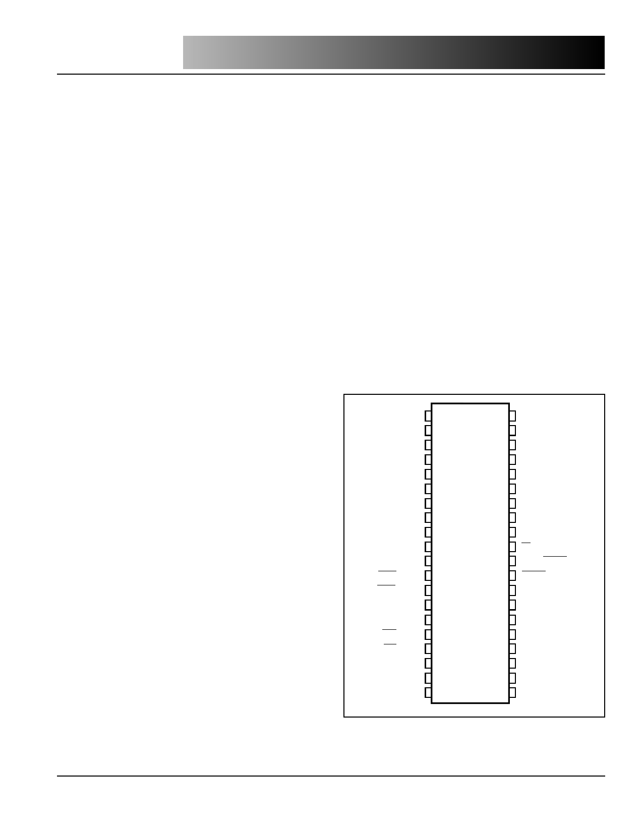
T2/P1.0
T2EX/P1.1
P1.2
P1.3
P1.4
P1.5
P1.6
P1.7
RST
RxD/P3.0
TxD/P3.1
INT0/P3.2
INT1/P3.3
T0/P3.4
T1/P3.5
WR/P3.6
RD/P3.7
XTAL2
XTAL1
GND
1
2
3
4
5
6
7
8
9
10
11
12
13
14
15
16
17
18
19
20
40 VCC
39 P0.0/AD0
38 P0.1/AD1
37 P0.2/AD2
36 P0.3/AD3
35 P0.4/AD4
34 P0.5/AD5
33 P0.6/AD6
32 P0.7/AD7
31 EA/VPP
30 ALE/PROG
29 PSEN
28 P2.7/A15
27 P2.6/A14
26 P2.5/A13
25 P2.4/A12
24 P2.3/A11
23 P2.2/A10
22 P2.1/A9
21 P2.0/A8
Figure 1. IS89C52 Pin Configuration: 40-pin PDIP
ISSI reserves the right to make changes to its products at any time without notice in order to improve design and supply the best possible product. We assume no responsibility for any errors which
may appear in this publication. © Copyright 1998, Integrated Silicon Solution, Inc.
Integrated Silicon Solution, Inc. — 1-800-379-4774
MC013-1C
11/21/98
1
1 page 
IS89C52
ISSI ®
Table 1. Detailed Pin Description
Symbol PDIP
ALE/PROG 30
PLCC
33
PQFP I/O
27 I/O
EA/VPP
31
35
29 I
P0.0-P0.7 39-32
43-36
37-30 I/O
P1.0-P1.7 1-8
2-9 40-44 I/O
1-3
P2.0-P2.7
1
2
21-28
2
3
24-31
40
41
18-25
I
I
I/O
Name and Function
Address Latch Enable: Output pulse for latching the low byte
of the address during an address to the external memory. In
normal operation, ALE is emitted at a constant rate of 1/6 the
oscillator frequency, and can be used for external timing or
clocking. Note that one ALE pulse is skipped during each
access to external data memory. This pin is also the Program
Pulse input (PROG) during Flash programming.
External Access enable: EA must be externally held low to
enable the device to fetch code from external program memory
locations 0000H to FFFFH. If EA is held high, the device
executes from internal program memory unless the program
counter contains an address greater than 0FFFH. This also
receives the 12V programming enable voltage (VPP) during
Flash programming.
Port 0: Port 0 is an 8-bit open-drain, bidirectional I/O port. Port
0 pins that have 1s written to them float and can be used as high-
impedance inputs. Port 0 is also the multiplexed low-order
address and data bus during accesses to external program and
data memory. In this application, it uses strong internal pullups
when emitting 1s.
Port 0 also receives the code bytes during programmable
memory programming and outputs the code bytes during
program verification. External pullups are required during pro-
gram verification.
Port 1: Port 1 is an 8-bit bidirectional I/O port with internal
pullups. Port 1 pins that have 1s written to them are pulled high
by the internal pullups and can be used as inputs. As inputs,
Port 1 pins that are externally pulled low will source current
because of the internal pullups. (See DC Characteristics: IIL).
The Port 1 output buffers can sink/source four TTL inputs.
Port 1 also receives the low-order address byte during Flash
programming and verification.
T2(P1.0): Timer/Counter 2 external count input.
T2EX(P1.1): Timer/Counter 2 trigger input.
Port 2: Port 2 is an 8-bit bidirectional I/O port with internal
pullups. Port 2 pins that have 1s written to them are pulled high
by the internal pullups and can be used as inputs. As inputs,
Port 2 pins that are externally pulled low will source current
because of the internal pullups. (See DC Characteristics: IIL).
Port 2 emits the high order address byte during fetches from
external program memory and during accesses to external data
memory that used 16-bit addresses (MOVX @ DPTR). In this
application, Port 2 uses strong internal pullups when emitting
1s. During accesses to external data memory that use 8-bit
addresses (MOVX @ Ri [i = 0, 1]), Port 2 emits the contents of
the P2 Special Function Register.
Port 2 also receives the high-order bits and some control
signals during Flash programming and verification. P2.6 and
P2.7 are the control signals while the chip programs and
erases.
Integrated Silicon Solution, Inc. — 1-800-379-4774
MC013-1C
11/21/98
5
5 Page 
IS89C52
ISSI ®
The detail description of each bit is as follows:
PSW:
Program Status Word. Bit Addressable.
IE:
Interrupt Enable Register. Bit Addressable.
765 4 3 2
CY AC F0 RS1 RS0 OV
10
—P
7 6 5 4 3 2 10
EA — — ES ET1 EX1 ET0 EX0
Register Description:
CY PSW.7 Carry flag.
AC PSW.6 Auxiliary carry flag.
F0 PSW.5 Flag 0 available to the user for g e n e r a l
purpose.
RS1 PSW.4 Register bank selector bit 1.(1)
RS0 PSW.3 Register bank selector bit 0.(1)
OV PSW.2 Overflow flag.
— PSW.1 Usable as a general purpose flag
P PSW.0 Parity flag. Set/Clear by hardware each
instruction cycle to indicate an odd/even
number of “1” bits in the accumulator.
Note:
1. The value presented by RS0 and RS1 selects the corre-
sponding register bank.
RS1 RS0 Register Bank
00
0
01
1
10
2
11
3
Address
00H-07H
08H-0FH
10H-17H
18H-1FH
PCON:
Power Control Register. Not Bit Addressable.
7 6 5 4 3 2 10
SMOD — — — GF1 GF0 PD IDL
Register Description:
SMOD
Double baud rate bit. If Timer 1 is used to generate
baud rate and SMOD=1, the baud rate is doubled
when the serial port is used in modes 1, 2, or 3.
— Not implemented, reserve for future use.(1)
— Not implemented, reserve for future use.(1)
— Not implemented, reserve for future use.(1)
GF1 General purpose flag bit.
GF0 General purpose flag bit.
PD Power-down bit. Setting this bit activates power-
down mode.
IDL Idle mode bit. Setting this bit activates idle mode.
If 1s are written to PD and IDL at the same time,
PD takes precedence.
Register Description:
EA IE.7
Disable all interrupts. If EA=0, no
interrupt will be acknowledged. If EA=1,
each interrupt source is individually
enabled or disabled by setting or
clearing its enable bit.
— IE.6
Not implemented, reserve for future
use.(5)
— IE.5
Not implemented, reserve for future
use.(5)
ES IE.4
Enable or disable the serial port
interrupt.
ET1 IE.3
Enable or disable the Timer 1 overflow
interrupt.
EX1 IE.2
Enable or disable External Interrupt 1.
ET0 IE.1
Enable or disable the Timer 0 overflow
interrupt.
EX0 IE.0
Enable or disable External Interrupt 0.
Note: To use any of the interrupts in the 80C51 Family, the
following three steps must be taken:
1. Set the EA (enable all) bit in the IE register to 1.
2. Set the coresponding individual interrupt enable bit in
the IE register to 1.
3. Begin the interrupt service routine at the corresponding
Vector Address of that interrupt (see below).
Interrupt Source
IE0
TF0
IE1
TF1
RI & TI
Vector Address
0003H
000BH
0013H
001BH
0023H
4. In addition, for external interrupts, pins INT0 and INT1
(P3.2 and P3.3) must be set to 1, and depending on
whether the interrupt is to be level or transition acti-
vated, bits IT0 or IT1 in the TCON register may need to
be set to 0 or 1.
ITX = 0 level activated (X = 0, 1)
ITX = 1 transition activated
5. User software should not write 1s to reserved bits. These
bits may be used in future products to invoke new
features.
Note:
1. User software should not write 1s to reserved bits. These
bits may be used in future products to invoke new features.
Integrated Silicon Solution, Inc. — 1-800-379-4774
MC013-1C
11/21/98
11
11 Page | ||
| Páginas | Total 50 Páginas | |
| PDF Descargar | [ Datasheet IS89C52-24PQI.PDF ] | |
Hoja de datos destacado
| Número de pieza | Descripción | Fabricantes |
| IS89C52-24PQ | CMOS SINGLE CHIP 8-BIT MICROCONTROLLER with 8-Kbytes of FLASH | Integrated Silicon Solution Inc |
| IS89C52-24PQI | CMOS SINGLE CHIP 8-BIT MICROCONTROLLER with 8-Kbytes of FLASH | Integrated Silicon Solution Inc |
| Número de pieza | Descripción | Fabricantes |
| SLA6805M | High Voltage 3 phase Motor Driver IC. |
Sanken |
| SDC1742 | 12- and 14-Bit Hybrid Synchro / Resolver-to-Digital Converters. |
Analog Devices |
|
DataSheet.es es una pagina web que funciona como un repositorio de manuales o hoja de datos de muchos de los productos más populares, |
| DataSheet.es | 2020 | Privacy Policy | Contacto | Buscar |