|
|
PDF IS61SP12832-150TQ Data sheet ( Hoja de datos )
| Número de pieza | IS61SP12832-150TQ | |
| Descripción | 128K x 32 SYNCHRONOUS PIPELINED STATIC RAM | |
| Fabricantes | ETC | |
| Logotipo |  |
|
Hay una vista previa y un enlace de descarga de IS61SP12832-150TQ (archivo pdf) en la parte inferior de esta página. Total 14 Páginas | ||
|
No Preview Available !
IS61SP12832
128K x 32 SYNCHRONOUS
PIPELINED STATIC RAM
FEATURES
• Internal self-timed write cycle
• Individual Byte Write Control and Global Write
• Clock controlled, registered address, data and
control
• Pentium™ or linear burst sequence control
using MODE input
• Three chip enables for simple depth expansion
and address pipelining
• Common data inputs and data outputs
• JEDEC 100-Pin LQFP and
119-pin PBGA package
• Single +3.3V, +10%, –5% power supply
• Power-down snooze mode
DESCRIPTION
The ICSI IS61SP12832 is a high-speed, low-power synchro-
nous static RAM designed to provide a burstable, high-perfor-
mance, secondary cache for the Pentium™, 680X0™, and
PowerPC™ microprocessors. It is organized as 131,072
words by 32 bits, fabricated with ICSI's advanced CMOS
technology. The device integrates a 2-bit burst counter, high-
speed SRAM core, and high-drive capability outputs into a
single monolithic circuit. All synchronous inputs pass through
registers controlled by a positive-edge-triggered single clock
input.
Write cycles are internally self-timed and are initiated by the
rising edge of the clock input. Write cycles can be from one to
four bytes wide as controlled by the write control inputs.
Separate byte enables allow individual bytes to be written.
BW1 controls DQa, BW2 controls DQb, BW3 controls DQc,
BW4 controls DQd, conditioned by BWE being LOW. A LOW
on GW input would cause all bytes to be written.
Bursts can be initiated with either ADSP (Address Status
Processor) or ADSC (Address Status Cache Controller) input
pins. Subsequent burst addresses can be generated internally
by the IS61SP12832 and controlled by the ADV (burst address
advance) input pin.
The mode pin is used to select the burst sequence order,
Linear burst is achieved when this pin is tied LOW. Interleave
burst is achieved when this pin is tied HIGH or left floating.
FAST ACCESS TIME
Symbol
Parameter
tKQ Clock Access Time
tKC Cycle Time
Frenquency
-166
3.5
6
166
-150
3.8
6.7
150
-133
4
7.5
133
-117
4
8.5
117
-5 Units
5 ns
10 ns
100 MHz
ICSI reserves the right to make changes to its products at any time without notice in order to improve design and supply the best possible product. We assume no responsibility for any errors
which may appear in this publication. © Copyright 2000, Integrated Circuit Solution Inc.
Integrated Circuit Solution Inc.
SSR011-0B
1
1 page 
IS61SP12832
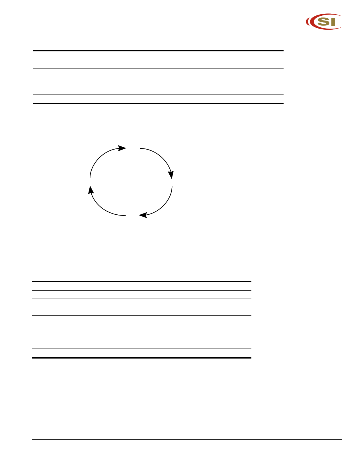
INTERLEAVED BURST ADDRESS TABLE (MODE = VCCQ or No Connect)
External Address
A1 A0
1st Burst Address
A1 A0
2nd Burst Address
A1 A0
3rd Burst Address
A1 A0
00 01 10 11
01 00 11 10
10 11 00 01
11 10 01 00
LINEAR BURST ADDRESS TABLE (MODE = GNDQ)
0,0
A1’, A0’ = 1,1
0,1
1,0
ABSOLUTE MAXIMUM RATINGS(1)
Symbol Parameter
Value
Unit
TBIAS Temperature Under Bias
TSTG
Storage Temperature
PD Power Dissipation
IOUT Output Current (per I/O)
VIN, VOUT Voltage Relative to GND for I/O Pins
VIN Voltage Relative to GND for
for Address and Control Inputs
–40 to +85
–55 to +150
1.6
100
–0.5 to VCCQ + 0.3
–0.5 to VCC + 0.5
°C
°C
W
mA
V
V
VCC
Voltage on Vcc Supply Relatiive to GND
–0.5 to 4.6
V
Notes:
1. Stress greater than those listed under ABSOLUTE MAXIMUM RATINGS may cause
permanent damage to the device. This is a stress rating only and functional operation of the
device at these or any other conditions above those indicated in the operational sections of
this specification is not implied. Exposure to absolute maximum rating conditions for
extended periods may affect reliability.
2. This device contains circuity to protect the inputs against damage due to high static voltages
or electric fields; however, precautions may be taken to avoid application of any voltage
higher than maximum rated voltages to this high-impedance circuit.
3. This device contains circuitry that will ensure the output devices are in High-Z at power up.
Integrated Circuit Solution Inc.
SSR011-0B
5
5 Page 
IS61SP12832
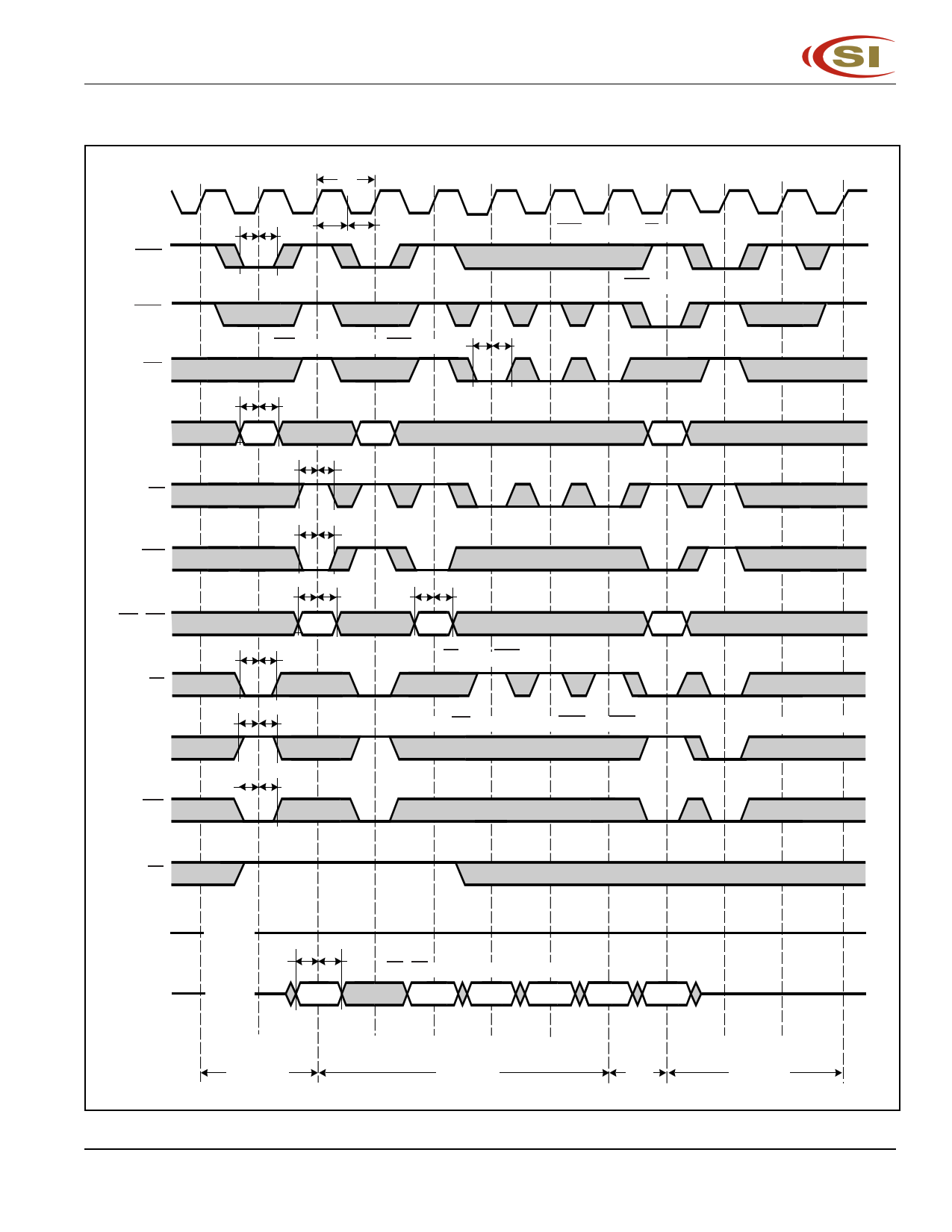
WRITE CYCLE TIMING
CLK
ADSP
ADSC
ADV
A16-A0
GW
BWE
BW4-BW1
CE
CE2
CE2
tKC
tKH
tSS tSH
tKL
ADV must be inactive for ADSP Write tAVS
tAS tAH
WR1
tWS
WR2
tWH
ADSP is blocked by CE inactive
ADSC initiate Write
tAVH
WR3
tWS tWH
tWS tWH
WR1
tWS tWH
WR2
tCES tCEH
CE Masks ADSP
WR3
tCES tCEH
CE2 and CE2 only sampled with ADSP or ADSC
tCES tCEH
Unselected with CE2
OE
DATAOUT
DATAIN
High-Z
tDS tDH BW4-BW1 only are applied to first cycle of WR2
High-Z 1a
2a 2b 2c 2d
3a
Single Write
Burst Write
Write Unselected
Integrated Circuit Solution Inc.
SSR011-0B
11
11 Page | ||
| Páginas | Total 14 Páginas | |
| PDF Descargar | [ Datasheet IS61SP12832-150TQ.PDF ] | |
Hoja de datos destacado
| Número de pieza | Descripción | Fabricantes |
| IS61SP12832-150TQ | 128K x 32 SYNCHRONOUS PIPELINED STATIC RAM | ETC |
| Número de pieza | Descripción | Fabricantes |
| SLA6805M | High Voltage 3 phase Motor Driver IC. |
Sanken |
| SDC1742 | 12- and 14-Bit Hybrid Synchro / Resolver-to-Digital Converters. |
Analog Devices |
|
DataSheet.es es una pagina web que funciona como un repositorio de manuales o hoja de datos de muchos de los productos más populares, |
| DataSheet.es | 2020 | Privacy Policy | Contacto | Buscar |
