|
|
|
PDF ispLSI8600V-60LB492 Data sheet ( Hoja de datos )
| Número de pieza | ispLSI8600V-60LB492 | |
| Descripción | 3.3V In-System Programmable SuperBIG High Density PLD | |
| Fabricantes | Lattice Semiconductor | |
| Logotipo | ||
Hay una vista previa y un enlace de descarga de ispLSI8600V-60LB492 (archivo pdf) en la parte inferior de esta página. Total 26 Páginas | ||
|
No Preview Available !
ispLSI® 8600V
3.3V In-System Programmable
SuperBIG™ High Density PLD
Features
• SuperBIG HIGH DENSITY IN-SYSTEM
PROGRAMMABLE LOGIC
— 3.3V Power Supply
— 32,000 PLD Gates/600 Macrocells
— 192-264 I/O Pins Supporting 3.3V/2.5V I/O
— 864 Registers
— High-Speed Global and Big Fast Megablock (BFM)
Interconnect
— Wide 20-Macrocell Generic Logic Block (GLB) for
High Performance
— Wide Input Gating (44 Inputs per GLB) for Fast
Counters, State Machines, Address Decoders, Etc.
— PCB-Efficient Ball Grid Array (BGA) Package
Options
• HIGH-PERFORMANCE E2CMOS® TECHNOLOGY
— fmax = 125 MHz Maximum Operating Frequency
— tpd = 8.5 ns Propagation Delay
— Electrically Erasable and Reprogrammable
— Non-Volatile
— Programmable Speed/Power Logic Path
Optimization
• IN-SYSTEM PROGRAMMABLE
— Increased Manufacturing Yields, Reduced Time-to-
Market and Improved Product Quality
— Reprogram Soldered Devices for Faster Debugging
• 100% IEEE 1149.1 BOUNDARY SCAN TESTABLE AND
3.3V IN-SYSTEM PROGRAMMABLE
• ARCHITECTURE FEATURES
— Enhanced Pin-Locking Architecture, Symmetrical
Generic Logic Blocks Connected by Hierarchical
Big Fast Megablock and Global Routing Planes
— Product Term Sharing Array Supports up to 28
Product Terms per Macrocell Output
— Macrocells Support Concurrent Combinatorial and
Registered Functions
— Embedded Tristate Bus Can Be Used as an Internal
Tristate Bus or as an Extension of an External
Tristate Bus
— Macrocell and I/O Registers Feature Multiple Control
Options, Including Set, Reset and Clock Enable
— I/O Pins Support Programmable Bus Hold, Pull-Up,
Open-Drain and Slew Rate Options
— Separate VCCIO Power Supply to Support 3.3V or
2.5V Input/Output Logic Levels
— I/O Cell Register Programmable as Input Register for
Fast Setup Time or Output Register for Fast Clock to
Output Time
• ispDesignEXPERT™ – LOGIC COMPILER AND COM-
PLETE ISP DEVICE DESIGN SYSTEMS FROM HDL
SYNTHESIS THROUGH IN-SYSTEM PROGRAMMING
— Superior Quality of Results
— Tightly Integrated with Leading CAE Vendor Tools
— Productivity Enhancing Timing Analyzer, Explore
Tools, Timing Simulator and ispANALYZER™
— PC and UNIX Platforms
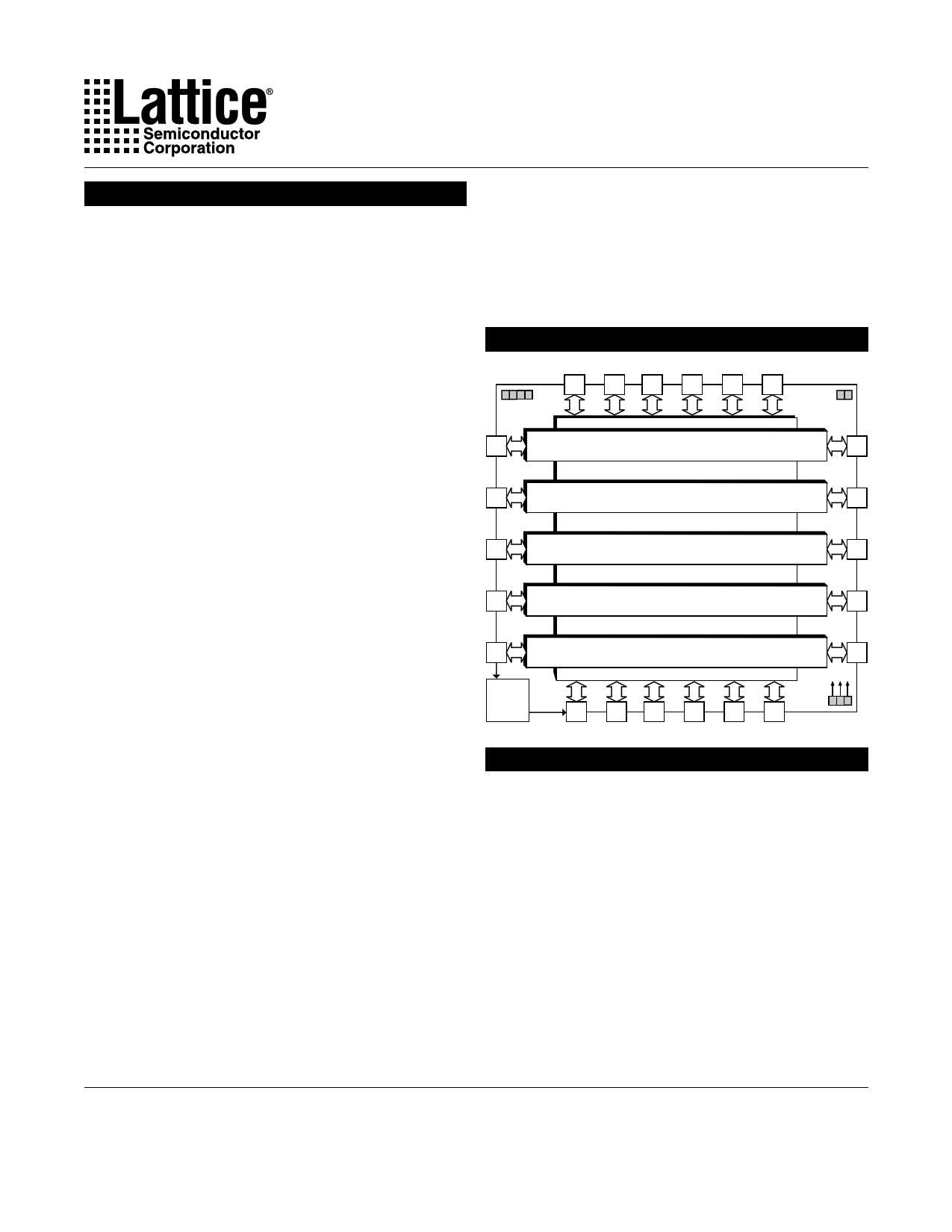
Functional Block Diagram
12 12 12 12 12 12
I/O I/O I/O I/O I/O I/O
12
I/O
Big Fast Megablock 0
12
I/O
12
I/O
Big Fast Megablock 1
12
I/O
12
I/O
Big Fast Megablock 2
Global Routing Plane
12
I/O
Big Fast Megablock 3
12
I/O
12
I/O
12
I/O
Big Fast Megablock 4
12
I/O
Boundary
Scan
12 12 12 12 12 12
I/O I/O I/O I/O I/O I/O
8600v block
ispLSI 8000V Family Description
The ispLSI 8000V Family of Register-Intensive, 3.3V
SuperBIG In-System Programmable Logic Devices is
based on Big Fast Megablocks of 120 registered macro-
cells and a Global Routing Plane (GRP) structure
interconnecting the Big Fast Megablocks. Each Big Fast
Megablock contains 120 registered macrocells arranged
in six groups of 20, a group of 20 being referred to as a
Generic Logic Block, or GLB. Within the Big Fast
Megablock, a Big Fast Megablock Routing Pool (BRP)
interconnects the six GLBs to each other and to 24 Big
Fast Megablock I/O cells with optional I/O registers. The
Global Routing Plane which interconnects the Big Fast
Megablocks has additional global I/Os with optional I/O
registers. The 192-I/O version contains 72 Big Fast
Megablock I/O and 120 global I/O, while the 264-I/O
Copyright © 2000 Lattice Semiconductor Corp. All brand or product names are trademarks or registered trademarks of their respective holders. The specifications and information herein are subject
to change without notice.
LATTICE SEMICONDUCTOR CORP., 5555 Northeast Moore Ct., Hillsboro, Oregon 97124, U.S.A.
July 2000
Tel. (503) 268-8000; 1-800-LATTICE; FAX (503) 268-8556; http://www.latticesemi.com
8600v_03
1
1 page 
Specifications ispLSI 8600V
Figure 2. ispLSI 8000V GLB Overview
I/O Big Fast Megablock Input Tracks
0
PT 0
PT 1
PT 2
PT 3
AND Array Input
Routing
General Purpose Big Fast Megablock Input Tracks
Feedback Inputs
43
20
Product Term
Sharing Array
PT 4
PT 5
PT 6
PT 7
PT 8
PT 9
PT 10
PT 11
PT 12
PT 13
PT 14
PT 15
Fully Populated
AND Array
Macrocell 0
From PTSA
PTSA Bypass
Single PT
PT Clock
PT Preset
PT Reset
Shared PT Clock
Bus Input
0
To Interconnect
Macrocell 1
From PTSA
PTSA Bypass
Single PT
PT Clock
PT Preset
PT Reset
Shared PT Clock
Bus Input
1
From Tristate
Bus Track
To Interconnect
Macrocell 2
From PTSA
PTSA Bypass
Single PT
PT Clock
PT Preset
PT Reset
Shared PT Clock
Bus Input
From Tristate
Bus Track
To Interconnect
2
Macrocell 3
From PTSA
PTSA Bypass
Single PT
PT Clock
PT Preset
PT Reset
Shared PT Clock
Bus Input
From Tristate
Bus Track
To interconnect
3
From Tristate
Bus Track
PT 76
PT 77
PT 78
PT 79
PT 80
PT 81
Note: Macrocells 9 and 10 do not support Tristate Bus Feedback.
5
Macrocell 19
From PTSA
PTSA Bypass
Single PT
PT Clock
PT Preset
PT Reset
Shared PT Clock
Bus Input
19
To Interconnect
From Tristate Bus Track
To Output Control MUX
Function Selector (E2 Cell Controlled)
5 Page 
Specifications ispLSI 8600V
Absolute Maximum Ratings 1,2
Supply Voltage Vcc .................................. -0.5 to +5.4V
Input Voltage Applied ............................... -0.5 to +5.6V
Tri-Stated Output Voltage Applied ........... -0.5 to +5.6V
Storage Temperature ................................ -65 to 150°C
Case Temp. with Power Applied .............. -55 to 125°C
Max. Junction Temp. (TJ) with Power Applied ... 150°C
1. Stresses above those listed under the “Absolute Maximum Ratings” may cause permanent damage to the device. Functional
operation of the device at these or at any other conditions above those indicated in the operational sections of this specification
is not implied (while programming, follow the programming specifications).
2. Compliance with the Thermal Management section of the Lattice Semiconductor Data Book or CD-ROM is a requirement.
DC Recommended Operating Condition
SYMBOL
VCC
VCCIO
Supply Voltage
I/O Supply Voltage
PARAMETER
Commercial TA = 0°C to 70°C
MIN.
3.0
2.3
MAX. UNITS
3.6 V
3.6 V
Table 2-0005/8600V
Capacitance (TA=25°C,f=1.0 MHz)
SYMBOL
C1
C2
C3
PARAMETER
I/O Capacitance
Clock Capacitance
Global Input Capacitance
TYPICAL
10
10
10
UNITS
pf
pf
pf
TEST CONDITIONS
VCC = 3.3V, VI/O = 2.0V
VCC = 3.3V, VCK = 2.0V
VCC = 3.3V, VG = 2.0V
Table 2-0006/8600V
Erase/Reprogram Specification
PARAMETER
Erase/Reprogram Cycles
MINIMUM
10000
MAXIMUM
–
UNITS
Cycles
Table 2-0008/8600V
11
11 Page | ||
| Páginas | Total 26 Páginas | |
| PDF Descargar | [ Datasheet ispLSI8600V-60LB492.PDF ] | |
Hoja de datos destacado
| Número de pieza | Descripción | Fabricantes |
| ispLSI8600V-60LB492 | 3.3V In-System Programmable SuperBIG High Density PLD | Lattice Semiconductor |
| Número de pieza | Descripción | Fabricantes |
| SLA6805M | High Voltage 3 phase Motor Driver IC. |
Sanken |
| SDC1742 | 12- and 14-Bit Hybrid Synchro / Resolver-to-Digital Converters. |
Analog Devices |
|
DataSheet.es es una pagina web que funciona como un repositorio de manuales o hoja de datos de muchos de los productos más populares, |
| DataSheet.es | 2020 | Privacy Policy | Contacto | Buscar |