|
|
|
PDF ispLSI2192VL-150LB144 Data sheet ( Hoja de datos )
| Número de pieza | ispLSI2192VL-150LB144 | |
| Descripción | 2.5V In-System Programmable SuperFAST High Density PLD | |
| Fabricantes | Lattice Semiconductor | |
| Logotipo | ||
Hay una vista previa y un enlace de descarga de ispLSI2192VL-150LB144 (archivo pdf) en la parte inferior de esta página. Total 13 Páginas | ||
|
No Preview Available !
ispLSI® 2192VL
2.5V In-System Programmable
SuperFAST™ High Density PLD
Features
• SuperFAST HIGH DENSITY IN-SYSTEM
PROGRAMMABLE LOGIC
— 8000 PLD Gates
— 96 I/O Pins, Nine Dedicated Inputs
— 192 Registers
— High Speed Global Interconnect
— Wide Input Gating for Fast Counters, State
Machines, Address Decoders, etc.
— Small Logic Block Size for Random Logic
— Pinout Compatible with ispLSI 2096V and 2096VE
• 2.5V LOW VOLTAGE ARCHITECTURE
— Interfaces with Standard 3.3V Devices (Inputs and
I/Os are 3.3V Tolerant)
— 175 mA Typical Active Current
• HIGH PERFORMANCE E2CMOS® TECHNOLOGY
— fmax = 150 MHz Maximum Operating Frequency
— tpd = 6.0 ns Propagation Delay
— Electrically Erasable and Reprogrammable
— Non-Volatile
— 100% Tested at Time of Manufacture
— Unused Product Term Shutdown Saves Power
• IN-SYSTEM PROGRAMMABLE
— 2.5V In-System Programmability (ISP™) Using
Boundary Scan Test Access Port (TAP)
— Open-Drain Output Option for Flexible Bus Interface
Capability, Allowing Easy Implementation of Wired-
OR Bus Arbitration Logic
— Increased Manufacturing Yields, Reduced Time-to-
Market and Improved Product Quality
— Reprogram Soldered Devices for Faster Prototyping
• 100% IEEE 1149.1 BOUNDARY SCAN TESTABLE
• THE EASE OF USE AND FAST SYSTEM SPEED OF
PLDs WITH THE DENSITY AND FLEXIBILITY OF FPGAS
— Enhanced Pin Locking Capability
— Three Dedicated Clock Input Pins
— Synchronous and Asynchronous Clocks
— Programmable Output Slew Rate Control
— Flexible Pin Placement
— Optimized Global Routing Pool Provides Global
Interconnectivity
• ispDesignEXPERT™ – LOGIC COMPILER AND COM-
PLETE ISP DEVICE DESIGN SYSTEMS FROM HDL
SYNTHESIS THROUGH IN-SYSTEM PROGRAMMING
— Superior Quality of Results
— Tightly Integrated with Leading CAE Vendor Tools
— Productivity Enhancing Timing Analyzer, Explore
Tools, Timing Simulator and ispANALYZER™
— PC and UNIX Platforms
Functional Block Diagram
Output Routing Pool
F7 F6 F5 F4 F3 F2 F1 F0
Output Routing Pool
E7 E6 E5 E4 E3 E2 E1 E0
A0
A1
A2
A3
Global Routing Pool (GRP)
A4
A5
A6
A7
DQ
DQ
Logic
Array D Q GLB
DQ
D7
D6
D5
D4
D3
D2
D1
D0
B0 B1 B2 B3 B4 B5 B6 B7
Output Routing Pool
C0 C1 C2 C3 C4 C5 C6 C7
Output Routing Pool
0139/2192VL
Description
The ispLSI 2192VL is a High Density Programmable
Logic Device containing 192 Registers, nine Dedicated
Input pins, three Dedicated Clock Input pins, two dedi-
cated Global OE input pins and a Global Routing Pool
(GRP). The GRP provides complete interconnectivity
between all of these elements. The ispLSI 2192VL fea-
tures in-system programmability through the Boundary
Scan Test Access Port (TAP) and is 100% IEEE 1149.1
Boundary Scan Testable. The ispLSI 2192VL offers non-
volatile reprogrammability of the logic, as well as the
interconnect to provide truly reconfigurable systems.
The basic unit of logic on the ispLSI 2192VL device is the
Generic Logic Block (GLB). The GLBs are labeled A0, A1
.. F7 (see Figure 1). There are a total of 48 GLBs in the
ispLSI 2192VL device. Each GLB is made up of four
macrocells. Each GLB has 18 inputs, a programmable
AND/OR/Exclusive OR array, and four outputs which can
be configured to be either combinatorial or registered.
Inputs to the GLB come from the GRP and dedicated
inputs. All of the GLB outputs are brought back into the
GRP so that they can be connected to the inputs of any
GLB on the device.
Copyright © 2000 Lattice Semiconductor Corp. All brand or product names are trademarks or registered trademarks of their respective holders. The specifications and information herein are subject
to change without notice.
LATTICE SEMICONDUCTOR CORP., 5555 Northeast Moore Ct., Hillsboro, Oregon 97124, U.S.A.
Tel. (503) 268-8000; 1-800-LATTICE; FAX (503) 268-8556; http://www.latticesemi.com
September 2000
2192vl_02
1
1 page 
Specifications ispLSI 2192VL
External Timing Parameters
Over Recommended Operating Conditions
PARAMETER
TEST 3
COND.
#
DESCRIPTION1
-150
-135
-100
UNITS
MIN. MAX. MIN. MAX. MIN. MAX.
tpd1
A 1 Data Propagation Delay, 4PT Bypass, ORP Bypass — 6.0 — 7.5 — 10.0 ns
tpd2
A 2 Data Propagation Delay
— 8.5 — 10.0 — 13.0 ns
fmax
A 3 Clock Frequency with Internal Feedback 2
150 — 135 — 100 — MHz
fmax (Ext.)
fmax (Tog.)
—
4
Clock
Frequency
with
External
Feedback
(1
tsu2 +
)tco1
111
—
95
— 77
— MHz
— 5 Clock Frequency, Max. Toggle
166 — 143 — 100 — MHz
tsu1
— 6 GLB Reg. Setup Time before Clock, 4 PT Bypass 4.0 — 5.0 — 6.5 — ns
tco1
A 7 GLB Reg. Clock to Output Delay, ORP Bypass
— 4.0 — 4.5 — 5.0 ns
th1
— 8 GLB Reg. Hold Time after Clock, 4 PT Bypass
0.0 — 0.0 — 0.0 — ns
tsu2
— 9 GLB Reg. Setup Time before Clock
5.0 — 6.0 — 8.0 — ns
tco2
A 10 GLB Reg. Clock to Output Delay
— 5.0 — 5.5 — 6.0 ns
th2 — 11 GLB Reg. Hold Time after Clock
0.0 — 0.0 — 0.0 — ns
tr1
A 12 Ext. Reset Pin to Output Delay, ORP Bypass
— 6.0 — 8.0 — 13.5 ns
trw1
— 13 Ext. Reset Pulse Duration
5.0 — 5.5 — 6.5 — ns
tptoeen
B 14 Input to Output Enable
— 10.0 — 12.0 — 15.0 ns
tptoedis
C 15 Input to Output Disable
— 10.0 — 12.0 — 15.0 ns
tgoeen
B 16 Global OE Output Enable
— 6.0 — 7.0 — 9.0 ns
tgoedis
C 17 Global OE Output Disable
— 6.0 — 7.0 — 9.0 ns
twh — 18 External Synchronous Clock Pulse Duration, High 3.0 — 3.5 — 5.0 — ns
twl — 19 External Synchronous Clock Pulse Duration, Low 3.0 — 3.5 — 5.0 — ns
1. Unless noted otherwise, all parameters use a GRP load of four, 20 PTXOR path, ORP and Y0 clock.
2. Standard 16-bit counter using GRP feedback.
3. Reference Switching Test Conditions section.
Table 2-0030C/2192VL
5
5 Page 
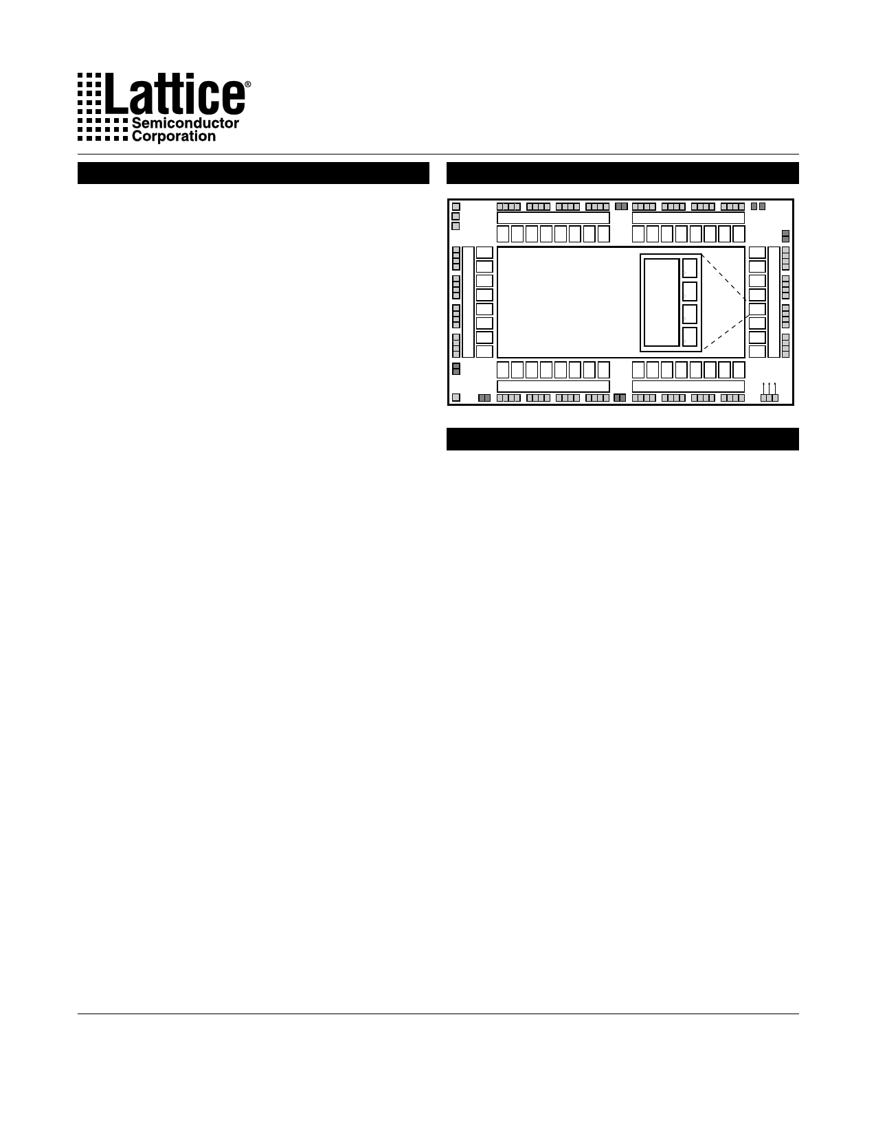
Pin Configuration
ispLSI 2192VL 128-Pin TQFP Pinout Diagram
Specifications ispLSI 2192VL
I/O 85
VCC
I/O 86
I/O 87
I/O 88
I/O 89
I/O 90
I/O 91
I/O 92
I/O 93
I/O 94
I/O 95
IN10
Y0
RESET
VCC
GOE 1
GND
BSCAN
TDI/IN 0
I/O 0
I/O 1
I/O 2
I/O 3
I/O 4
I/O 5
I/O 6
I/O 7
I/O 8
I/O 9
VCC
I/O 10
1
2
3
4
5
6
7
8
9
10
11
12
13
14
15
16
17
18
19
20
21
22
23
24
25
26
27
28
29
30
31
32
ispLSI 2192VL
Top View
96 I/O 58
95 VCC
94 I/O 57
93 I/O 56
92 I/O 55
91 I/O 54
90 I/O 53
89 I/O 52
88 I/O 51
87 I/O 50
86 I/O 49
85 I/O 48
84 IN 8
83 Y1
82 IN4
81 VCC
80 GOE 0
79 GND
78 Y2
77 TCK/IN 7
76 I/O 47
75 I/O 46
74 I/O 45
73 I/O 44
72 I/O 43
71 I/O 42
70 I/O 41
69 I/O 40
68 I/O 39
67 I/O 38
66 VCC
65 I/O 37
0124-2192VL
11
11 Page | ||
| Páginas | Total 13 Páginas | |
| PDF Descargar | [ Datasheet ispLSI2192VL-150LB144.PDF ] | |
Hoja de datos destacado
| Número de pieza | Descripción | Fabricantes |
| ispLSI2192VL-150LB144 | 2.5V In-System Programmable SuperFAST High Density PLD | Lattice Semiconductor |
| Número de pieza | Descripción | Fabricantes |
| SLA6805M | High Voltage 3 phase Motor Driver IC. |
Sanken |
| SDC1742 | 12- and 14-Bit Hybrid Synchro / Resolver-to-Digital Converters. |
Analog Devices |
|
DataSheet.es es una pagina web que funciona como un repositorio de manuales o hoja de datos de muchos de los productos más populares, |
| DataSheet.es | 2020 | Privacy Policy | Contacto | Buscar |