|
|
|
PDF IspLSI2032E-225LJ44 Data sheet ( Hoja de datos )
| Número de pieza | IspLSI2032E-225LJ44 | |
| Descripción | In-System Programmable SuperFAST High Density PLD | |
| Fabricantes | Lattice Semiconductor | |
| Logotipo | ||
Hay una vista previa y un enlace de descarga de IspLSI2032E-225LJ44 (archivo pdf) en la parte inferior de esta página. Total 14 Páginas | ||
|
No Preview Available !
ispLSI® 2032E
In-System Programmable
SuperFAST™ High Density PLD
Features
Functional Block Diagram
• SuperFAST HIGH DENSITY IN-SYSTEM
PROGRAMMABLE LOGIC
— 1000 PLD Gates
— 32 I/O Pins, Two Dedicated Inputs
— 32 Registers
— High Speed Global Interconnect
— Wide Input Gating for Fast Counters, State
Machines, Address Decoders, etc.
— Small Logic Block Size for Random Logic
— 100% Functionally and JEDEC Upward Compatible
with ispLSI 2032 Devices
• HIGH PERFORMANCE E2CMOS® TECHNOLOGY
— fmax = 225 MHz Maximum Operating Frequency
— tpd = 3.5 ns Propagation Delay
— TTL Compatible Inputs and Outputs
— 5V Programmable Logic Core
— ispJTAG™ In-System Programmable via IEEE 1149.1
(JTAG) Test Access Port
— User-Selectable 3.3V or 5V I/O (48-Pin Package Only)
Supports Mixed Voltage Systems
— PCI Compatible Outputs (48-Pin Package Only)
— Open-Drain Output Option
— Electrically Erasable and Reprogrammable
— Non-Volatile
— Unused Product Term Shutdown Saves Power
• ispLSI OFFERS THE FOLLOWING ADDED FEATURES
— Increased Manufacturing Yields, Reduced Time-to-
Market and Improved Product Quality
— Reprogram Soldered Devices for Faster Prototyping
• OFFERS THE EASE OF USE AND FAST SYSTEM
SPEED OF PLDs WITH THE DENSITY AND FLEXIBILITY
OF FIELD PROGRAMMABLE GATE ARRAYS
— Complete Programmable Device Can Combine Glue
Logic and Structured Designs
— Enhanced Pin Locking Capability
— Three Dedicated Clock Input Pins
— Synchronous and Asynchronous Clocks
— Programmable Output Slew Rate Control to
Minimize Switching Noise
— Flexible Pin Placement
— Optimized Global Routing Pool Provides Global
Interconnectivity
• ispDesignEXPERT™ – LOGIC COMPILER AND COM-
PLETE ISP DEVICE DESIGN SYSTEMS FROM HDL
SYNTHESIS THROUGH IN-SYSTEM PROGRAMMING
— Superior Quality of Results
— Tightly Integrated with Leading CAE Vendor Tools
— Productivity Enhancing Timing Analyzer, Explore
Tools, Timing Simulator and ispANALYZER™
— PC and UNIX Platforms
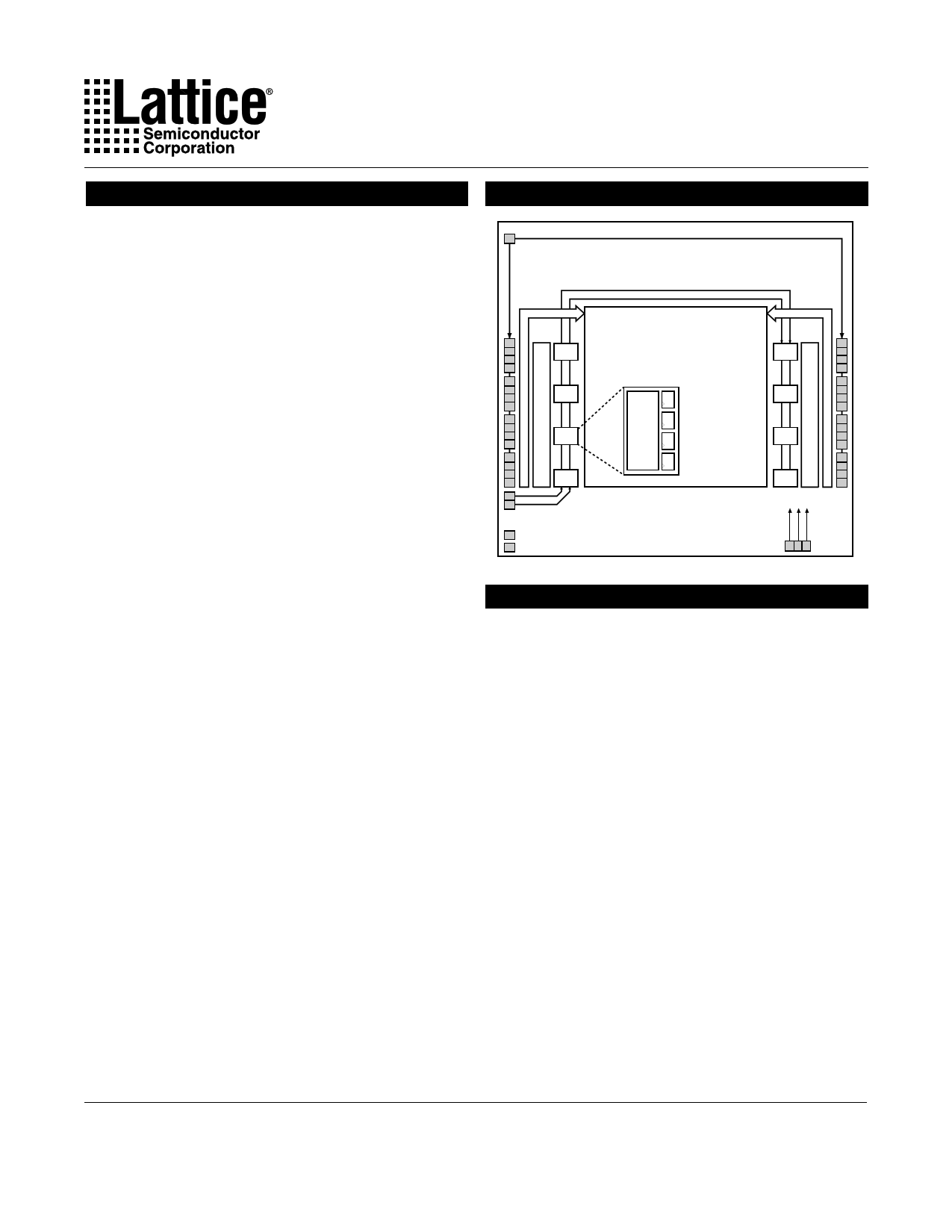
A0
Global Routing Pool
(GRP)
A1
A2 GLB
A3
DQ
Logic D Q
Array D Q
DQ
A7
A6
A5
A4
0139Bisp/2000
Description
The ispLSI 2032E is a High Density Programmable Logic
Device. The device contains 32 Registers, 32 Universal
I/O pins, two Dedicated Input Pins, three Dedicated
Clock Input Pins, one dedicated Global OE input pin and
a Global Routing Pool (GRP). The GRP provides com-
plete interconnectivity between all of these elements.
The ispLSI 2032E features 5V in-system programmabil-
ity and in-system diagnostic capabilities. The ispLSI
2032E offers non-volatile reprogrammability of the logic,
as well as the interconnect to provide truly reconfigurable
systems.
The basic unit of logic on the ispLSI 2032E device is the
Generic Logic Block (GLB). The GLBs are labeled A0, A1
.. A7 (see Figure 1). There are a total of eight GLBs in the
ispLSI 2032E device. Each GLB is made up of four
macrocells. Each GLB has 18 inputs, a programmable
AND/OR/Exclusive OR array, and four outputs which can
be configured to be either combinatorial or registered.
Inputs to the GLB come from the GRP and dedicated
inputs. All of the GLB outputs are brought back into the
GRP so that they can be connected to the inputs of any
GLB on the device.
The device also has 32 I/O cells, each of which is directly
connected to an I/O pin. Each I/O cell can be individually
Copyright © 1999 Lattice Semiconductor Corp. All brand or product names are trademarks or registered trademarks of their respective holders. The specifications and information herein are subject
to change without notice.
LATTICE SEMICONDUCTOR CORP., 5555 Northeast Moore Ct., Hillsboro, Oregon 97124, U.S.A.
June 1999
Tel. (503) 268-8000; 1-800-LATTICE; FAX (503) 268-8556; http://www.latticesemi.com
2032e_03
1
1 page 
Specifications ispLSI 2032E
External Timing Parameters
Over Recommended Operating Conditions
PARAMETER
TEST
COND.4
#2
DESCRIPTION1
-225
-200
-180
UNITS
MIN. MAX. MIN. MAX. MIN. MAX.
tpd1
A 1 Data Prop. Delay, 4PT Bypass, ORP Bypass – 3.5 – 3.5 – 5.0 ns
tpd2
A 2 Data Prop. Delay
– 5.5 – 5.5 – 7.5 ns
fmax
A 3 Clk Frequency with Int. Feedback3
225 – 200 – 180 – MHz
fmax (Ext.)
fmax (Tog.)
–
4
Clk
Frequency
with
Ext.
Feedback
(
1
tsu2 +
)tco1
167 – 167 – 125 –
MHz
– 5 Clk Frequency, Max. Toggle
250 – 250 – 200 – MHz
tsu1
– 6 GLB Reg. Setup Time before Clk, 4 PT Bypass 2.5 – 2.5 – 3.0 – ns
tco1
A 7 GLB Reg. Clk to Output Delay, ORP Bypass
– 2.5 – 2.5 – 4.0 ns
th1 – 8 GLB Reg. Hold Time after Clk, 4 PT Bypass 0.0 – 0.0 – 0.0 – ns
tsu2
– 9 GLB Reg. Setup Time before Clk
3.5 – 3.5 – 4.0 –
ns
tco2
– 10 GLB Reg. Clk to Output Delay
– 3.5 – 3.5 – 4.5 ns
th2 – 11 GLB Reg. Hold Time after Clk
0.0 – 0.0 – 0.0 –
ns
tr1 A 12 Ext. Reset Pin to Output Delay, ORP Bypass – 5.0 – 5.0 – 6.5 ns
trw1
– 13 Ext. Reset Pulse Duration
3.5 – 3.5 – 4.0 –
ns
tptoeen
B 14 Input to Output Enable
– 7.0 – 7.0 – 10.0 ns
tptoedis
C 15 Input to Output Disable
– 7.0 – 7.0 – 10.0 ns
tgoeen
B 16 Global OE Output Enable
– 3.5 – 3.5 – 5.0 ns
tgoedis
C 17 Global OE Output Disable
– 3.5 – 3.5 – 5.0 ns
twh
– 18 Ext. Synch. Clk Pulse Duration, High
2.0 – 2.0 – 2.5 –
ns
twl
– 19 Ext. Synch. Clk Pulse Duration, Low
2.0 – 2.0 – 2.5 –
ns
1. Unless noted otherwise, all parameters use a GRP load of four GLBs, 20 PTXOR path, ORP and Y0 clock.
2. Refer to Timing Model in this data sheet for further details.
3. Standard 16-bit counter using GRP feedback.
4. Reference Switching Test Conditions section.
Table 2-0030A/2032E
5
5 Page 
Specifications ispLSI 2032E
Pin Description
NAME
I/O 0 - I/O 3
I/O 4 - I/O 7
I/O 8 - I/O 11
I/O 12 - I/O 15
I/O 16 - I/O 19
I/O 20 - I/O 23
I/O 24 - I/O 27
I/O 28 - I/O 31
44-PIN PLCC
PIN NUMBERS
15, 16, 17, 18,
19, 20, 21, 22,
25, 26, 27, 28,
29, 30, 31, 32,
37, 38, 39, 40,
41, 42, 43, 44,
3, 4, 5, 6,
7, 8, 9, 10
44-PIN TQFP
PIN NUMBERS
9, 10, 11, 12,
13, 14, 15, 16,
19, 20, 21, 22,
23, 24, 25, 26,
31 32, 33, 34,
35, 36, 37, 38,
41, 42, 43, 44,
1, 2, 3, 4
48-PIN TQFP
PIN NUMBERS
9, 10, 11, 13,
14, 15, 16, 17,
20, 21, 22, 23,
25, 26, 27, 28,
33, 34, 35, 37,
38, 39, 40, 41,
44, 45, 46, 47,
1, 2, 3, 4
DESCRIPTION
Input/Output Pins — These are the general purpose
I/O pins used by the logic array.
GOE 0
2
40 43 Global Output Enable input pin.
Y0 11 5 5 Dedicated Clock input. This clock input is connected to
one of the clock inputs of all the GLBs on the device.
RESET/Y1
35
29
31 This pin performs two functions:
- Dedicated clock input. This clock input is brought
into the Clock Distribution Network, and can optionally
be routed to any GLB and/or I/O cell on the device.
- Active Low (0) Reset pin which resets all of the GLB
and I/O registers in the device.
BSCAN
TDI/IN 01
13
14
TMS/NC2
TDO/IN 11
TCK/Y21
36
24
33
GND
1, 23
7
8
30
18
27
17, 39
7
8
32
19
29
12, 18, 36, 42
Input — Dedicated in-system programming enable
input pin. This pin is brought low to enable the
programming mode. The TMS, TDI, TDO and TCK
controls become active.
Input — This pin performs two functions. When
BSCAN is logic low, it functions as an input pin to load
programming data into the device. TDI/IN0 also is used
as one of the two control pins for the ISP state
machine. When BSCAN is high, it functions as a
dedicated input pin.
Input — When in ISP mode, controls operation of ISP
state machine.
Output/Input — This pin performs two functions. When
BSCAN is logic low, it functions as an output pin to
read serial shift register data. When BSCAN is high, it
functions as a dedicated input pin.
Input — This pin performs two functions. When
BSCAN is logic low, it functions as a clock pin for the
Serial Shift Register. When BSCAN is high, it
functions as a dedicated clock input. This clock input
is brought into the Clock Distribution Network and
can be routed to any GLB and/or I/O cell on the
device.
Ground (GND)
VCC
VCCIO
12, 34
6, 28
6, 30
24, 48
1. Pins have dual function capability.
2. NC pins are not to be connected to any active signals, VCC or GND.
VCC
Supply voltage for output drivers, 5V or 3.3V. All
VCCIO pins must be connected to the same voltage
level.
Table 2-0002/2032E
11
11 Page | ||
| Páginas | Total 14 Páginas | |
| PDF Descargar | [ Datasheet IspLSI2032E-225LJ44.PDF ] | |
Hoja de datos destacado
| Número de pieza | Descripción | Fabricantes |
| ispLSI2032E-225LJ44 | In-System Programmable SuperFAST High Density PLD | Lattice Semiconductor |
| ISPLSI2032E-225LJ44 | In-System Programmable SuperFAST High Density PLD | Lattice Semiconductor |
| IspLSI2032E-225LJ44 | In-System Programmable SuperFAST High Density PLD | Lattice Semiconductor |
| Número de pieza | Descripción | Fabricantes |
| SLA6805M | High Voltage 3 phase Motor Driver IC. |
Sanken |
| SDC1742 | 12- and 14-Bit Hybrid Synchro / Resolver-to-Digital Converters. |
Analog Devices |
|
DataSheet.es es una pagina web que funciona como un repositorio de manuales o hoja de datos de muchos de los productos más populares, |
| DataSheet.es | 2020 | Privacy Policy | Contacto | Buscar |