|
|
|
PDF ispGDX160A-5Q208 Data sheet ( Hoja de datos )
| Número de pieza | ispGDX160A-5Q208 | |
| Descripción | In-System Programmable Generic Digital CrosspointTM | |
| Fabricantes | Lattice Semiconductor | |
| Logotipo | ||
Hay una vista previa y un enlace de descarga de ispGDX160A-5Q208 (archivo pdf) en la parte inferior de esta página. Total 25 Páginas | ||
|
No Preview Available !
ispGDXTM Family
In-System Programmable
Generic Digital CrosspointTM
Features
Functional Block Diagram
• IN-SYSTEM PROGRAMMABLE GENERIC DIGITAL
CROSSPOINT FAMILY
— Advanced Architecture Addresses Programmable
PCB Interconnect, Bus Interface Integration and
Jumper/Switch Replacement
— Three Device Options: 80 to 160 Programmable I/O
Pins
— “Any Input to Any Output” Routing
— Fixed HIGH or LOW Output Option for Jumper/DIP
Switch Emulation
— Space-Saving TQFP, PQFP and BGA Packaging
— Dedicated IEEE 1149.1-Compliant Boundary Scan
Test
— PCI Compliant Output Drive
• HIGH PERFORMANCE E2CMOS® TECHNOLOGY
— 5V Power Supply
— 5.0ns Input-to-Output/5.0ns Clock-to-Output Delay
— Low-Power: 40mA Quiescent Icc
— Balanced 24mA Output Buffers with Programmable
Slew Rate Control
— Schmitt Trigger Inputs for Noise Immunity
— Electrically Erasable and Reprogrammable
— Non-Volatile E2CMOS Technology
— 100% Tested
• ispGDX OFFERS THE FOLLOWING ADVANTAGES
— In-System Programmable
— Lattice ISP or JTAG Programming Interface
— Only 5V Power Supply Required
— Change Interconnects in Seconds
— Reprogram Soldered Devices
• FLEXIBLE ARCHITECTURE
— Combinatorial/Latched/Registered Inputs or Outputs
— Individual I/O Tri-state Control with Polarity Control
— Dedicated Clock Input Pins (two or four) or
Programmable Clocks from I/O Pins (from 20 up to
40)
— Up to 4:1 Dynamic Path Selection
— Programmable Output Pull-up Resistors
— Outputs Tri-state During Power-up (“Live Insertion”
Friendly)
• DESIGN SUPPORT THROUGH LATTICE’S ispGDX
DEVELOPMENT SOFTWARE
— MS Windows or NT / PC-Based or Sun O/S
— Easy Text-Based Design Entry
— Automatic Signal Routing
— Program up to 100 ISP Devices Concurrently
— Simulator Netlist Generation for Easy Board-Level
Simulation
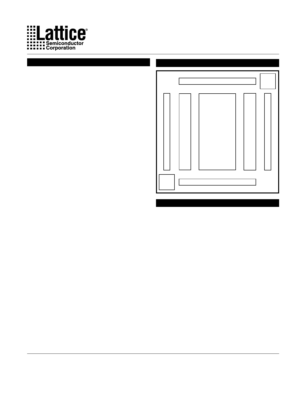
I/O Pins D
ISP
Control
I/O
Cells
Global Routing
Pool
(GRP)
I/O
Cells
Boundary
Scan
Control
I/O Pins B
Description
The ispGDX architecture provides a family of fast, flexible
programmable devices to address a variety of system-
level digital signal routing and interface requirements
including:
• Multi-Port Multiprocessor Interfaces
• Wide Data and Address Bus Multiplexing
(e.g. 4:1 High-Speed Bus MUX)
• Programmable Control Signal Routing
(e.g. Interrupts, DMAREQs, etc)
• Board-Level PCB Signal Routing for Prototyping or
Programmable Bus Interfaces
The ispGDX Family consists of three members with 80,
120 and 160 Programmable I/Os. These devices are
available in packages ranging from the 100-pin TQFP to
the 208-pin PQFP. The devices feature fast operation,
with input-to-output signal delays (Tpd) of 5ns and clock-
to-output delays of 5ns.
The architecture of the devices consists of a series of
programmable I/O cells interconnected by a Global Rout-
Copyright © 2000 Lattice Semiconductor Corporation. All brand or product names are trademarks or registered trademarks of their respective holders. The specifications and information herein
are subject to change without notice.
LATTICE SEMICONDUCTOR CORP., 5555 Northeast Moore Ct., Hillsboro, Oregon 97124, U.S.A.
Tel. (503) 268-8000; 1-800-LATTICE; FAX (503) 268-8556; http://www.latticesemi.com
August 2000
ispgdx_08
1
1 page 
Specifications ispGDX Family
Applications (Cont.)
Figure 3. Address Demultiplex/Data Buffering
XCVR
I/OA I/OB
OEA OEB
Address
Latch
DQ
CLK
Buffered
Data
To Memory/
Peripherals
Address
Figure 4. Data Bus Byte Swapper
D0-7
XCVR
I/OA I/OB
OEA OEB
D8-15
XCVR
I/OA I/OB
OEA OEB
D0-7
XCVR
I/OA I/OB
OEA OEB
D8-15
XCVR
I/OA I/OB
OEA OEB
Figure 5. Four-Port Memory Interface
4-to-1
16-Bit MUX
Bidirectional
Port #1
OE1
Memory
Port
Port #2
OE2
OEM
Port #3
OE3
SEL0
Port #4
OE4
SEL1
To
Memory
Designing with the ispGDX
As mentioned earlier, this architecture satisfies the PRSI
class of applications without restrictions: any I/O pin as a
single input or bidirectional can drive any other I/O pin as
output.
For the case of PDP applications, the designer does have
to take into consideration the limitations on pins that can
be used as control (MUX0, MUX1, OE, CLK) or data
(MUXA-D) inputs. The restrictions on control inputs are
not likely to cause any major design issues because the
input possibilities span 25% of the total pins.
The MUXA-D input partitioning requires that designers
consciously assign pinouts so that MUX inputs are in the
appropriate, disjoint groups. For example, since the
MUXA group includes I/O0-19 (80 I/O device), it is not
possible to use I/O0 and I/O9 in the same MUX function.
As previously discussed, data path functions will be
assigned early in the design process and these restric-
tions are reasonable in order to optimize speed and cost.
User Electronic Signature
The ispGDX Family includes dedicated User Electronic
Signature (UES) E2CMOS storage to allow users to code
design-specific information into the devices to identify
particular manufacturing dates, code revisions, or the
like. The UES information is accessible through the
boundary scan or Lattice ISP programming port via a
specific command. This information can be read even
when the security cell is programmed.
Security Bit
The ispGDX Family includes a security bit feature that
prevents reading the device program once set. Even
when set, it does not inhibit reading the UES or device ID
code. It can be erased only via a device bulk erase.
Note: All OE and SEL lines driven by external arbiter logic (not shown).
5
5 Page 
Specifications ispGDX Family
ispGDX Development System
The ispGDX Development System supports ispGDX
design using a simple language syntax and an easy-to-
use Graphical User Interface (GUI) called Design
Manager. From creation to In-System Programming, the
ispGDX system is an easy-to-use, self-contained design
tool delivered on CD-ROM media.
Windows 95 and Windows NT. When the ispGDX
software is invoked, the Design Manager and an accom-
panying message window are displayed. The Design
Manager consists of the Menu Bar, Tool Bar, Status Bar
and the work area. The figure below shows these
elements of the ispGDX GUI.
Features
• Easy-to-use Text Entry System
• ispGDX Design Compiler
- Design Rule Checker
- I/O Connectivity Checker
- Automatic Compiler Function
• Industry Standard JEDEC File for Programming
• Min / Max Timing Report
• Interfaces To Popular Timing Simulators
• User Electronic Signature (UES) Support
• Detailed Log and Report Files For Easy Design Debug
• On-Line Help
• Windows 3.1x, WIN95, and NT Compatible Graphical
User Interface
• SUN O/S, Command Line Driven version available
The Menu Bar displays topics related to functions used in
the design process. Access the various drop-down
menus and submenus by using the mouse or “hot” keys.
The menu items available in the ispGDX system are
FILE, EDIT, DEVICE, INVOKE, INTERFACES, VIEW,
WINDOW and HELP.
The Tool Bar is a quick and easy way to perform many of
the functions found in the menus with a single click of the
mouse. File, Edit, Undo, Redo, Find, Print Download and
Compiler are just some of the Icons found in the ispGDX
Tool Bar. For instance, the Compiler Icon performs the
same function as the Invoke => Compiler menu com-
mands, including design analysis and rule checking and
the fitting operation.
The Status Bar displays action prompts and the line and
column numbers reflect the location of the cursor within
the message window or the work area.
Workstation Version
PC Version
With the ispGDX GUI for the PC, command line entry is
not required. The tools run under Microsoft Windows 3.1,
Lattice's ispGDX Development System Interface
The ispGDX software is also available for use under the
Sun O/S 4.1.x or Solaris 2.4 or 2.5. The Sun version of
the ispGDX software is invoked from the command line
under the UNIX operating system. A GUI is not sup-
ported in this environment.
In the UNIX environment, the ispGDX Design File (GDF)
must be created using a text editor. Once the GDF has
been created, invoke the ispGDX workstation software
from the UNIX command line. The following is an ex-
ample of how to invoke ispGDX software.
Usage:
ispGDX
[-i input_file]
[-of[edif|orcad|viewlogic|verilog|vhdl]]
[-p part name]
[-r par_file]
-i input_file name
ispGDX design file
-of [edif | orcad | viewlogic | verilog | vhdl]
output format
-p part_name
ispGDX part number
-r par_file
read parameters from parameter file
11
11 Page | ||
| Páginas | Total 25 Páginas | |
| PDF Descargar | [ Datasheet ispGDX160A-5Q208.PDF ] | |
Hoja de datos destacado
| Número de pieza | Descripción | Fabricantes |
| ispGDX160A-5Q208 | In-System Programmable Generic Digital CrosspointTM | Lattice Semiconductor |
| Número de pieza | Descripción | Fabricantes |
| SLA6805M | High Voltage 3 phase Motor Driver IC. |
Sanken |
| SDC1742 | 12- and 14-Bit Hybrid Synchro / Resolver-to-Digital Converters. |
Analog Devices |
|
DataSheet.es es una pagina web que funciona como un repositorio de manuales o hoja de datos de muchos de los productos más populares, |
| DataSheet.es | 2020 | Privacy Policy | Contacto | Buscar |