|
|
|
PDF ISL6590DR Data sheet ( Hoja de datos )
| Número de pieza | ISL6590DR | |
| Descripción | Digital Multi-Phase PWM Controller for Core-Voltage Regulation | |
| Fabricantes | Intersil Corporation | |
| Logotipo | ||
Hay una vista previa y un enlace de descarga de ISL6590DR (archivo pdf) en la parte inferior de esta página. Total 24 Páginas | ||
|
No Preview Available !
®
Data Sheet
April 2003
ISL6590
FN9061
Digital Multi-Phase PWM Controller for
Core-Voltage Regulation
Processors that operate above a GHz require fast, intelligent
power systems. The Intersil ISL6590 controller offers
intelligent digital, multi-phase control that provides high
bandwidth, optimal control frequency response, noise
immunity and active transient response control algorithms.
The design is fully scalable for controlling up to six phases,
each featuring the Intersil ISL6580 intelligent power stage.
The user can configure and monitor the power system via
the Asynchronous Serial Interface (ASI). The ISL6590
controller flexibility can be extended with the addition of an
external EEPROM for updating key circuit operating
parameters in the control loop and overall system design.
The digital architecture reduces the design time for
engineers with the use of our software. The software allows
the designer the freedom to choose output stage
components and still achieve optimized system
performance.
The ISL6590 digital controller communicates with the
ISL6580 integrated power stages via 100% digital signaling.
Serial communication allows for separation of the controller
and the power stage, providing placement and layout
freedom to the power stage. The digital controller
implements phase balancing to ensure even distribution of
phase currents. The ISL6590 controller configures the
ISL6580 power stage current limit, VID reference, non-
overlap period, Active Transient Response (ATR) trigger
levels and maximum temperature limit. The digital controller
also monitors the ISL6580 power stage peak currents, over-
temperature fault, input under voltage, output over/under
voltage to ensure proper operation of the power supply.
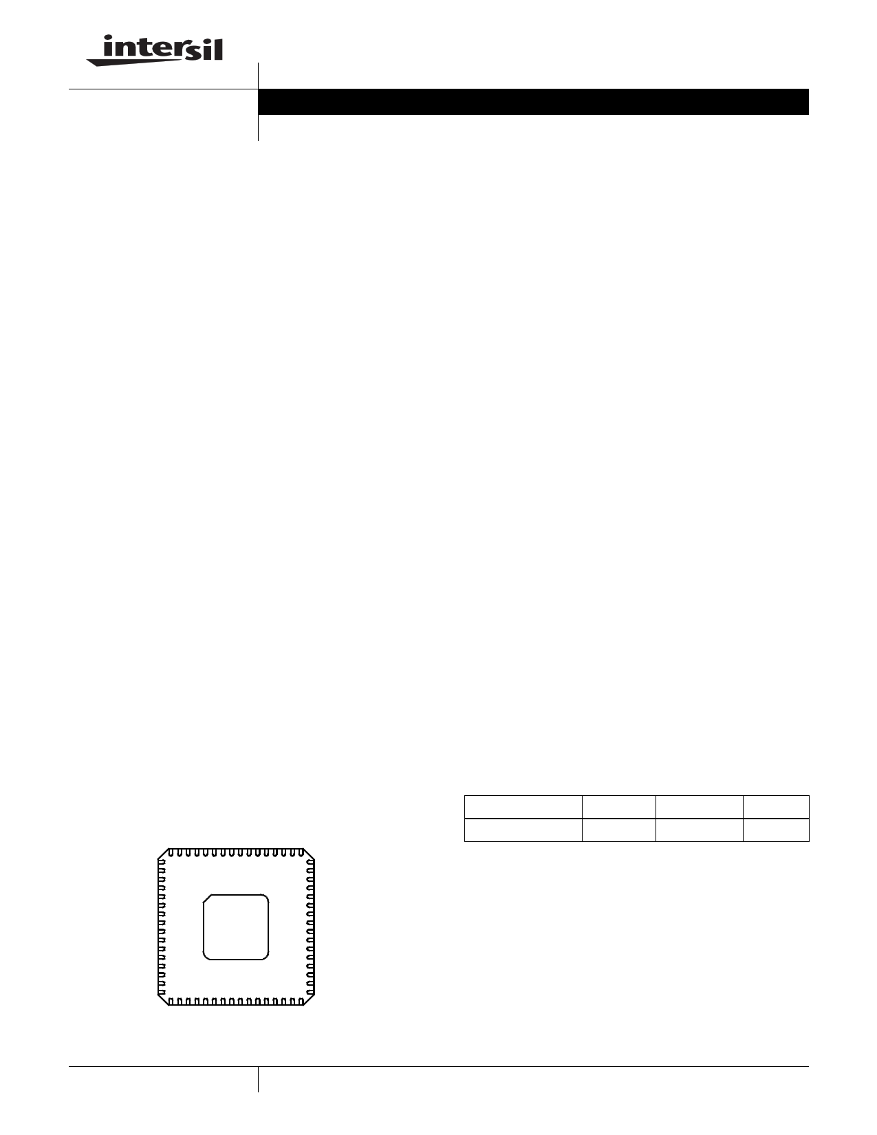
Pinout
ISL6590 (QFN)
TOP VIEW
OUTEN
VID [0]
VID [1]
VID [2]
VID [3]
VID [4]
VID [5]
VDD_CORE
PWRGD
VDD_IO
MCLK
MDO
MDI
MCS
NDRIVE1
PWM1
64
01
16
17
49
48
TEST 2
ATRL
SOC
ERR
VDD_IO
SYS_CLK
VDD_IO
NC
NC
VDD_CORE
NC
NC
IDIG6
PWM6
NDRIVE6
33
32
TEST1
Features
• Open Architecture features software programmable
control loop compensation enabling optimal system
performance
- User accessible asynchronous serial interface
• Intel VR10
- 6-bit Dynamic VID™
- Output voltage regulation range of 0.8375V to 1.600Vdc
• 250kHz to 1MHz switching frequency
• 100% digital control and signaling
• Active Transient Response (ATR) control algorithms for
minimized voltage droop and overshoot
• Controls up to six ISL6580 intelligent power stages (20A
per phase, 120A total system current)
• Programmable Adaptive voltage positioning (AVP) load
line
• Configurable control loop parameters (with optional
external EEPROM)
• Programmable MOSFET dead time control
• High speed voltage and current control loops
• PWRGD and OUTEN
• Serial interface to ISL6580 power stages for system
monitoring and configuration
• 64 Ld 9x9 QFN package
• QFN Package Option
- QFN Compliant to JEDEC PUB95 MO-220 QFN - Quad
Flat No Leads - Product Outline
- QFN Near Chip Scale Package Footprint; Improves
PCB Efficiency, Thinner in Profile.
Ordering Information
PART NUMBER TEMP. (oC) PACKAGE PKG. NO.
ISL6590DR
0 to 85 64 Ld 9x9 QFN L64.9x9-S
1 CCAUTION: These devices are sensitive to electrostatic discharge; follow proper IC Handling Procedures.
1-888-INTERSIL or 321-724-7143 | Intersil (and design) is a registered trademark of Intersil Americas Inc.
Copyright © Intersil Americas Inc. 2003. All Rights Reserved
All other trademarks mentioned are the property of their respective owners. Dynamic VID™ is a trademark of Intersil Americas Inc.
1 page 
ISL6590
Pin Descriptions
PIN NO.
1
PIN NAME
OUTEN
2-7
8, 21, 39, 57
9
VID[0:5]
VDD_CORE
PWRGD
10, 25, 42,
44, 54
11
VDD_IO
MCLK
12
13
14
15, 18, 22,
26, 30, 34
16, 19, 23,
27, 31, 35
17, 20, 24,
28, 32, 36
MDO
MDI
MCS
NDRIVE[1:6]
PWM[1:6]
IDIG[1:6]
29
33, 48, 50,
51
37, 38, 40,
41
43
EXT_Reset
TEST[1:4]
NC
SYSCLK
45 ERR
46 SOC
47 ATRL
49 ATRH
52 SDATA
53 SCLK
55 ATX
56 ARX
58 OSC_OUT
59 OSC_IN
60 PLL_DIG_VSS
PLL Bypass
61 PLL_DIG_VDD
62 PLL_ANA_VSS
63 PLL_ANA_VDD
64 PLL_Filter
65 GND
TYPE
Input
Input
Power
Output
Power
PIN DESCRIPTION
Output enable high input signal used to command the regulator on and a low input signal turns
the regulator off.
Voltage identification (6 bit). Programs Vout regulation voltage.
IC internal core supply voltage (1.8 VDC logic).
Power Good high output signal to indicate the regulator output voltage is within the specified
range. A low signal indicates the voltage is not within range.
IC I/O input supply voltage (3.3 VDC logic).
Output
Output
Input
Output
Output
EEPROM external memory clock, data is clocked out of the IC on the rising edge and data is
clocked into the ISL6580 IC on the falling edge. Compliant with SPI™ EEPROMs.
EEPROM external memory data output. Compliant with SPI EEPROMs.
EEPROM external memory data input. Compliant with SPI EEPROMs.
EEPROM external memory chip select (Active low). Compliant with SPI EEPROMs.
Low side drive signal used to initiate the ISL6580 to turn on the LSFET.
Output PWM performs pulse width modulation which is used to turn on the ISL6580’s power devices.
Input
Input
Output
Current A/D data serial 7-bit digital word (MSB first). The first bit is a start bit (Start = 1). The
remaining 6 bits represent the sampled peak current in the drain of the particular ISL6580
P-Channel HSFET. (IDIG word transmission is triggered by the falling edge of the PWM signal.)
IDIG is an input that is received at SYSCLK/2, normally 66.6MHz.
Voltage identification (6 bit). Programs Vout regulation voltage.
Test pins for part evaluation
N/A These pins have not been bonded out.
Input/Output System clock which runs at a 133.3MHz rate used to clock the ISL6580. This is generated by the
internal PLL circuit to create a 4x frequency multiply of the OSC_IN frequency.
Input
Serial data transmitted at a 66MHz (or SYSCLK/2) rate. This 6 bit voltage error is feedback into
the control loop and used to regulate the output voltage.
Input
Start of Conversion signal initiated by the ISL6580’s Voltage A/D to create the ERR signal.
Input
Active Transient Response Low input signal from the ISL6580 indicating a voltage overshoot on
the converter output.
Input
Active Transient Response High input signal from the ISL6580 indicating a voltage droop on the
converter output.
Input/Output Controller serial interface for communication, monitoring, and configuration data between the
ISL6580 and ISL6590 controller.
Output
Serial digital bus clock supplied for the 16.67MHz clocking that accompanies SDATA via the
Backside serial bus.
Output Asynchronous Serial Interface Transmit
Input
Asynchronous Serial Interface Receive
Output Only used if part is using a crystal to generate the system clock.
Input
Ground
Input
Requires a 33.33MHz oscillator or crystal which is used to generate system clock.
Digital Ground for the 4X clock multiplier PLL.
Test mode to bypass PLL input to core.
Power 1.8V power supply for the 4X clock multiplier PLL clock tree driver (1.8 VDC logic).
Ground Analog Ground for the 4X clock multiplier PLL.
Power 1.8V power supply for the 4X clock multiplier PLL (1.8 VDC logic).
Analog Input Filter cap for PLL.
Ground Paddle IC Ground
5
5 Page 
ISL6590
the status register which then allows accesses to the Non-
Volatile Memory map.
ISL6590 Data Write Timing
SCLK
SDATA
Tp
t DSU
tDH
tKH
FIGURE 6. ISL6590 DATA WRITE TIMING
tSPH
FIGURE 4. EEPROM DATA READ TIMING
TABLE 6. EEPROM DATA READ TIMING
TIMING NAME PARAMETER
MIN
UNITS
Data Setup
Data Hold
tDSU
tDH
20 ns
20 ns
TABLE 8. DATA WRITE TIMING
TIMING NAME PARAMETER TYPICAL
Data Setup
Data Hold
Kick Hold
Stop Hold
SCLK Period
tDSU
tDH
tKH
tSPH
tp
45
15
15
15
62.5
ISL6590 Data Read Timing
UNITS
ns
ns
ns
ns
ns
FIGURE 5. EEPROM DATA WRITE TIMING
TABLE 7. EEPROM TIMING
TIMING NAME PARAMETER TYPICAL
CS to MCLK delay
Data Setup
Data Hold
Clock Period
MCLK to CS delay
tCSSU
tDSU
tDH
tP
tCSH
480
240
240
480
720
UNITS
ns
ns
ns
ns
ns
Write-Through Cycles
During startup and local register loading, any incoming
writecycles to the Non-Volatile Memory will be held off until
start up and configuration is complete. During normal
operation, writes to the Non-Volatile Memory shall be
extended until such time that the data is both written to and
read back from the external EEPROM.
FIGURE 7. DATA READ TIMING
TABLE 9. DATA READ TIMING
TIMING NAME PARAMETER TYPICAL
Data Setup
Data Hold
tDSU
tDH
52
14
UNITS
ns
ns
11
11 Page | ||
| Páginas | Total 24 Páginas | |
| PDF Descargar | [ Datasheet ISL6590DR.PDF ] | |
Hoja de datos destacado
| Número de pieza | Descripción | Fabricantes |
| ISL6590DR | Digital Multi-Phase PWM Controller for Core-Voltage Regulation | Intersil Corporation |
| Número de pieza | Descripción | Fabricantes |
| SLA6805M | High Voltage 3 phase Motor Driver IC. |
Sanken |
| SDC1742 | 12- and 14-Bit Hybrid Synchro / Resolver-to-Digital Converters. |
Analog Devices |
|
DataSheet.es es una pagina web que funciona como un repositorio de manuales o hoja de datos de muchos de los productos más populares, |
| DataSheet.es | 2020 | Privacy Policy | Contacto | Buscar |